Posted on Leave a comment

Quantum LTO2 CL1001 Tape Drive Teardown

Drive Top
Drive Top

I have recently begun to create an archive of all my personal data, and since LTO2 tape drives offer significant capacity (200GB/400GB) per tape, longevity is very high (up to 30 years in archive), & relatively low cost, this is the technology I’ve chosen to use for my long term archiving needs.

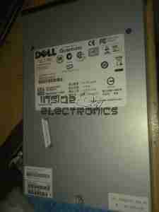
Unfortunately, this drive was DOA, due to being dropped in shipping. This drop broke the SCSI LVD connector on the back of the unit, & bent the frame, as can be seen below.
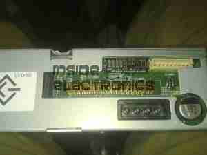
Broken SCSI
Broken SCSI

As this drive is unusable, it made for a good teardown candidate.
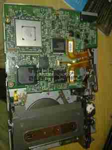
Cover Removed
Cover Removed

Here the top cover of the drive has been removed, showing the top of the main logic PCB. The large silver IC in the top corner is the main CPU for the drive. It’s a custom part, but it does have an ARM core.

The two Hitachi ICs are the R/W head interface chipset, while the smaller LSI IC is the SCSI controller.
The tape transport & loading mech can be seen in the lower half of the picture.
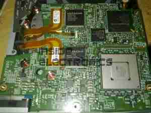
Main Logic
Main Logic

Close up of the main logic.

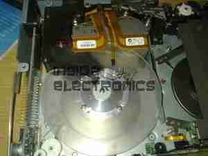
Tape Spool
Tape Spool

Here the main logic PCB has been removed, showing the tape take up spool. The data cartridges have only one spool to make the size smaller. When the tape is loaded, the drive grabs onto the leader pin at the end of the tape & feeds it onto this spool.
The head assembly is just above the spool.
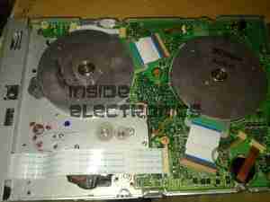
Bottom Plate Removed

Bottom of the drive with the cover plate removed. Here the spindle drive motors are visible, both brushless 3-Phase units. Both of these motors are driven by a single controller IC on the other side of the lower logic PCB.
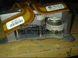
Head Drive Motor
Head Drive Motor

The head is moved up & down the face of the tape by this stepper motor for coarse control, while fine control is provided by a voice coil assembly buried inside the head mount.
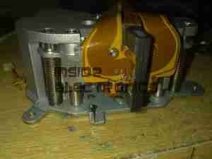
Tape Head Assembly
Tape Head Assembly

The face of the tape R/W head. This unit contains 2 sets of 8 heads, one of which writes to the tape, the other then reads the written data back right after to verify integrity.
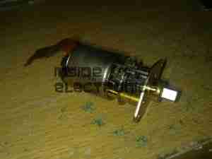
Cartridge Load Motor

The tape cartridge loading motor. I originally thought that this was a standard brushed motor, but it has a ribbon cable emerging, this must be some sort of brushless arrangement.

A replacement drive is on the way, I shall be documenting some more of my archiving efforts & system setup once that unit arrives.
Posted on 1 Comment

Superhub Buffer Overflow?

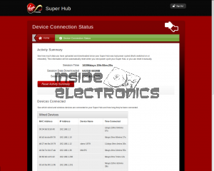
While checking my Virgin Media-provided router recently, I came across this in the status page:

How Many Days??
How Many Days??

According to this, it seems to think it’s been running for a grand total of 44.8 years, without a reboot. I’m pretty certain that DOCSIS didn’t exist that long ago, let alone the hardware itself…
Tech Fail

Posted on Leave a comment

ZyXel WAP3205 Repair

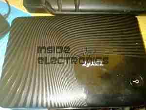
Here is a ZyXel WAP3205 WiFi Access Point that has suffered a reverse polarity event, due to an incorrect power supply being used with the unit.

ZyXEL WAP3205
ZyXEL WAP3205

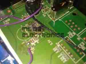
While most electronic gadgets are protected against reverse polarity with a blocking diode, this unit certainly wasn’t. Applying +12v DC the wrong way round resulted in this:

Blown Switchmode IC
Blown Switchmode IC (Fuzzy Focus)

That is the remains of the 3.3v regulator IC, blown to smithereens & it even attempted an arson attack. Luckily this was the only damaged component, & I was able to repair the unit by replacing the switching IC with a standalone regulator. (Replacing the IC would have been preferable, if there was anything left of it to obtain a part number from).

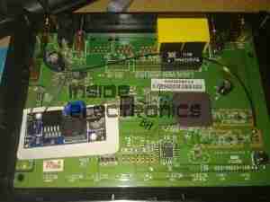
I scraped away the pins of the IC to clear the short on the input supply, removed the switching inductor, & tacked on an adjustable regulator module set to 3.3v. Luckily the voltage of the supply is handily marked on the PCB next to the circuit.

Replacement PSU
Replacement PSU

Replacement SMPS in place on top of the PCB. The output of the supply is connected to one of the pads of L4 (on my unit just an 0 ohm link), the +12v input is connected to the + rail side of C8 & C7 & the final ground connection is hooked in to the back of the barrel jack.

After this replacement, the unit booted straight up as if nothing had happened. All the logic is undamaged!

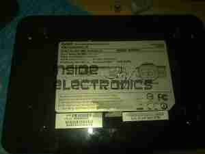
Makerplate
Makerplate
Posted on Leave a comment

uRadMonitor Network

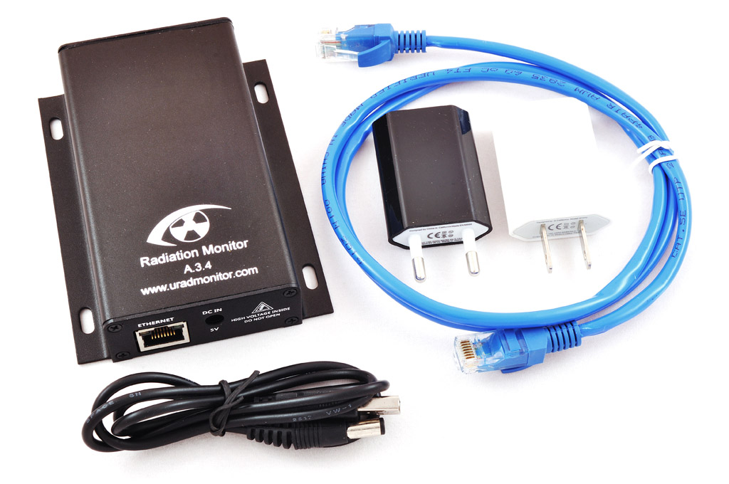
I’ve joined the uRadMonitor network! I’m told my unit is on the way & it should be going live here in Manchester, UK within about 10 days.

uRadMonitor Unit
uRadMonitor Unit

This is a crowd project to monitor background radiation levels all over the world, so far there’s a lot of units already online.

More to come once my unit arrives!

Posted on Leave a comment

LDR Controlled Relay

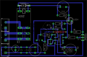
Here’s a quick project for nightlight use: an LDR controlled relay.

Powered from 12v DC, this circuit uses an LM311 comparator to switch the relay according to the sensitivity set by the potentiometer.

LDR Relay
LDR Relay

Eagle files can be downloaded below.

[download id=”5577″]

Posted on Leave a comment

AD9850 VFO Board

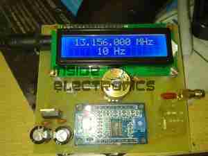
Continuing from my previous post where I published an Eagle design layout for AD7C‘s Arduino powered VFO, here is a completed board.

I have made some alterations to the design since posting, which are reflected in the artwork download in that post, mainly due to Eagle having a slight psychotic episode making me ground one of the display control signals!

AD9850 VFO
AD9850 VFO

The amplifier section is unpopulated & bypassed as I was getting some bad distortion effects from that section, some more work is needed there.
The Arduino Pro Mini is situated under the display, and the 5v rail is provided by the LM7805 on the lower left corner.

Current draw at 12v input is 150mA, for a power of 1.8W total. About 1W of this is dissipated in the LM7805 regulator, so I have also done a layout with an LM2574 Switching Regulator.
The SMPS version should draw a lot let power, as less is being dissipated in the power supply, but this version is more complex.

DDS VFO-SMPS
DDS VFO-SMPS

Here the SMPS circuit can be seen on the left hand side of the board, completely replacing the linear regulator.
I have not yet built this design, so I don’t know what kind of effect this will have on the output signal, versus the linear regulator. I have a feeling that the switching frequency of the LM2574 (52kHz) might produce some interference on the output of the DDS module. However I have designed this section to the standards in the datasheet, so this should be minimal.

Nevertheless this version is included in the Downloads section at the bottom of this post.

The output coupled through a 100nF capacitor is very clean, as can be seen below, outputting a 1kHz signal. Oscilloscope scale is 0.5ms/div & 1V/div.

VFO Output
VFO Output (Mucky ‘Scope)
Scope Connected
Scope Connected


Thanks again to Rich over at AD7C for the very useful tool design!

Linked below is the Eagle design files for this project, along with my libraries used to create it.

[download id=”5571″]

[download id=”5573″]

[download id=”5575″]

Posted on 4 Comments

AD9850 DDS VFO PCB & Schematic Layout

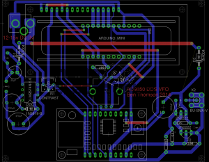
I recently came across a design for an Arduino controlled AD9850 DDS module, created by AD7C, so I figured I would release my Eagle CAD design for the PCB here.

It is a mainly single-sided layout, only a few links on the top side are needed so this is easy to etch with the toner transfer method.

My version uses an Arduino Pro Mini, as the modular format is much easier to work with than a bare ATMega 328.

RF output is via a SMA connector & has a built in amplifier to compensate for the low level generated by the DDS Module.

DDS VFO
DDS VFO

Version 2 Update: Added reverse polarity protection, added power indicator LED, beefed up tracks around the DC Jack.
[download id=”5571″]