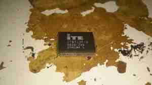
These chips are used on PC motherboards, to control many of the legacy peripherals & things such as temperature monitoring & fan speed control.
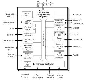
Here’s the block diagram from the datasheet to show all the features, this IC handles many things on a modern motherboard!


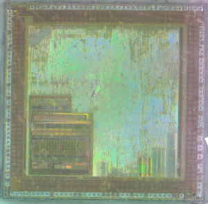
Very interesting decap, thanks for sharing. The IC certainly looks I/O bound vs. the node used for the internal chiplets at least. I would be interested to hear the die size and any other details you can share on what we are looking at. Public documentation on these ICs is pretty sparse as to the internal implementation. They all seem to reference an 8042-based keyboard controller, but few details beyond that. I do know there were some FDD controllers and serial controllers based on the 8048 as well. Looking at this, I wonder if it is all done with a single fast 8048 derivative plus a few add ons.