Since I do my own PCBs on a somewhat regular basis, I decided it was time to move to a more professional method to etch my boards. I have been using the cheap toner transfer method, using special yellow coated paper from China. (I think it’s coated in wax, or some plastic film).
The toner transfer paper does usually work quite well, but I’ve had many issues with pinholes in the transfer, which cause the etched tracks to look horrid, (not to mention the potential for breaks & reduced current capacity), and the toner not transferring properly at all, to issues with the paper permanently fusing to the copper instead of just transferring the toner.
BigClive has done a couple of fairly comprehensive videos on the dry film photoresist available from AliExpress & eBay. This stuff is used similarly to the toner transfer method, in that the film is fused to the board with heat, but then things diverge. It’s supplied either in cut sheets, or by the roll. I ordered a full roll to avoid the issues I’ve heard of when the stuff is folded in the post – once it’s creased, it’s totally useless. The dry film itself is a gel sandwiched between two protective plastic film sheets, and bonds to the board with the application of heat from a laminator.
The board is first cleaned with scotchbrite pad & soap to remove any tarnish & oil from the copper.
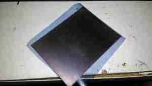
Once the board has been cleaned, one side of the backing film is removed from the gel with adhesive tape, and the dry film is placed on the board while still wet. This stops the film from sticking immediately to the clean copper, one edge is pressed down, and it’s then fed through a modified laminator:
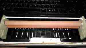
I’ve cut away most of the plastic covering the hot rollers, as constant jamming was an issue with this cheapo unit. All the mains power is safely tucked away under some remaining plastic cover at the end. The board with it’s covering of dry film is fed into the laminator – the edge that was pressed down first. This allows the laminator to squeeze out any remaining water & air bubbles from between the two so no creases or blisters form.
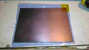
Once the board has been run through the laminator about 6 times, (enough to get it very hot to the touch), the film is totally bonded to the copper. The top film is left in place to protect the UV sensitive layer during expsure.
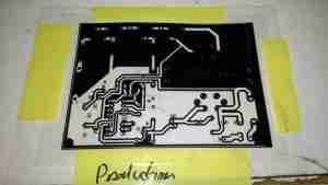
The exposure mask is laser printed onto OHP transparencies, in this case I’ve found I need to use two copies overlaid to get enough opacity in the black toner sections to block the UV light. Some touching up with a Sharpie is also easy to do if there are any weak spots in the toner coverage. This film is negative type – All the black areas will be unexposed and washed off in the developer tank. I also found I had to be fairly generous with track spacing, using too small lines just causes issues with the UV curing bits of film it isn’t supposed to.
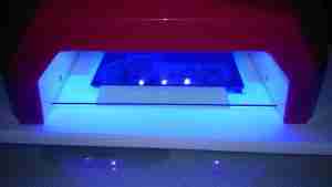
The PCB is placed on a firm surface, the exposure mask lined up on top, and the whole thing covered with a sheet of standard glass to apply even pressure. The UV exposure lamp in this case is a cheap eBay UV nail curing unit, with 15 high power LEDs. (I’ll do a teardown on this when I get some time, it’s got some very odd LEDs in it). Exposing the board for 60 seconds is all the time needed.
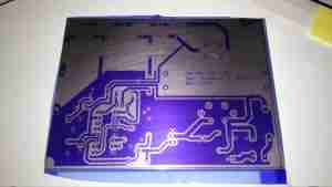
After the board is exposed, the areas that got hit with the UV light have turned purple – the resist has hardened in these areas. It’s bloody tough as well, I’ve scrubbed at it with some vigour and it doesn’t come off. Toner transfer was a bit naff in this respect, most of the time the toner came off so easily that the etchant lifted it off. After this step is done, the remaining protective film on the top can be removed.
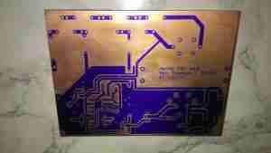
The film is developed in a solution of Sodium Carbonate (washing Soda). This is mildly alkaline and it dissolves off the unexposed resist.
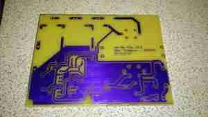
Now it’s into the etching tank for a couple of minutes, I’m still using Ferric Chloride to etch my boards, at about 60°C. Etching at room temperature is much too slow. Once this is done, the board is washed, and then dipped in the strip tank for a couple of minutes. This is a Sodium Hydroxide solution, and is very caustic, so gloves are required for this bit. Getting Ferric Chloride on skin is also a fairly bad idea, it stains everything orange, and it attacks pretty much every metal it comes into contact with, including Stainless Steel.
This method does require some more effort than the toner transfer method, but it’s much more reliable. If something goes wrong with the exposure, it’s very easy to strip the board completely & start again before etching. This saves PCB material and etchant. This is definitely more suited to small-scale production as well, since the photomask can be reused, there’s much less waste at the end. The etched lines are sharper, much better defined & even with some more chemicals involved, it’s a pretty clean process. All apart from the Ferric Chloride can be disposed of down the sink after use, since the developer & stripper are just alkaline solutions.

Bueno. Yo tengo un serio problema con las láminas de dry film photoresist. Parece que están pasadas de tiempo, ya que las compré por sBay en 2017 y no las utilizaba desde entonces hasta ahora. El problema es que ambas (una que le compré a un ruso, y la otra en puesto de ventas por eBay a un chino) me están dañando el trabajo porque cuando las expongo bajo un cecador de uñas, se ve que se muestran las pistas en la película de vinilo o de lo que estén hechas estas photoresist cecas. Pero cuando las paso al revelador en líquido, se desprenden de la placa de cobre dejando solamente una mancha en la superficie de la placa muy parecida a la enfermedad de la piel llamada “paño” o empeine. No me atrevo a pasarla por el percloruro férrico porque dudo que destruya todo el cobre de la placa y la deje totalmente lisa y se pierda lo que trato de hacer.
Estoy buscando información para saber si el dry film photoresist tiene fecha de vencimiento y no encuentro quién me lo diga. Por favor, si ya has pasado por una experiencia similar a esta, escríbeme a mi email un mensaje eficaz que me dé la aclaración del tema y a la vez, que sirva de mucho para otras personas del área que tal vez estén pasando cosa como esta por la que yo estoy pasando. Mi gran duda es que no sé qué hacer al respecto, si confiar en las dry film photoresist o quizas buscar el método que estás mencionando que no te dio buenos resultados. Es como una avenida por la que vamos viajando muchas personas, unas que van y otras que vienen.