Since I wrote the post about the RF SWR & Power meter, I’ve been meaning to get around to a redesign of the board with a built-in directional coupler, and that time has finally come.

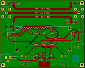
So, here’s what I came up with. It’s pretty much the same as the first version on the acquisition & digital sections, but now there’s a built in directional coupler at the top edge of the board. Footprints are provided for N-Type connectors for the RF section. The effective length of the coupler is about 78mm, with 3mm wide tracks, with 2.8mm separation between the transmission line & the pickup lines.

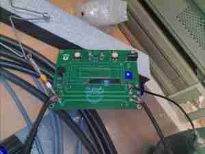
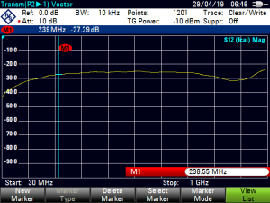
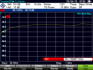
A quick turnaround from JLCPCB gave me some prototype PCBs to play with, and above I have a test board set up on a Network Analyser. I’ve got the unused parts terminated at 50Ω, and this gave me the following plots:

The response is pretty flat across the range at about -25dB coupling, rolling off at about 200MHz at the bottom end due to the relatively short length of the coupler. There’s a bit of a dip at ~700MHz, but I suspect that is down to one of the test cables used.

The reverse power coupler gives a very similar result, with the 700MHz+ dip going in reverse. I suspect things aren’t that perfect due to the coupler tracks not being quite symmetrical. Revision 2.2 of the board should give me some slightly better results.
Stay tuned for the next iteration!
73s, 2E0GXE

I was looking for design help on directional couplers and stumbled onto your site. Very nice indeed! Lot’s of entertaining teardowns and other work.
Did you ever get around to making revision 2.2 of this board? Also, I was wondering how you arrived at the coupler design?
Hi… nice design. What sort of directivity were you able to achieve?
Looks like the PCB may have been done in KICAD. If so any chance of getting a copy please?
Cheers,
Graham