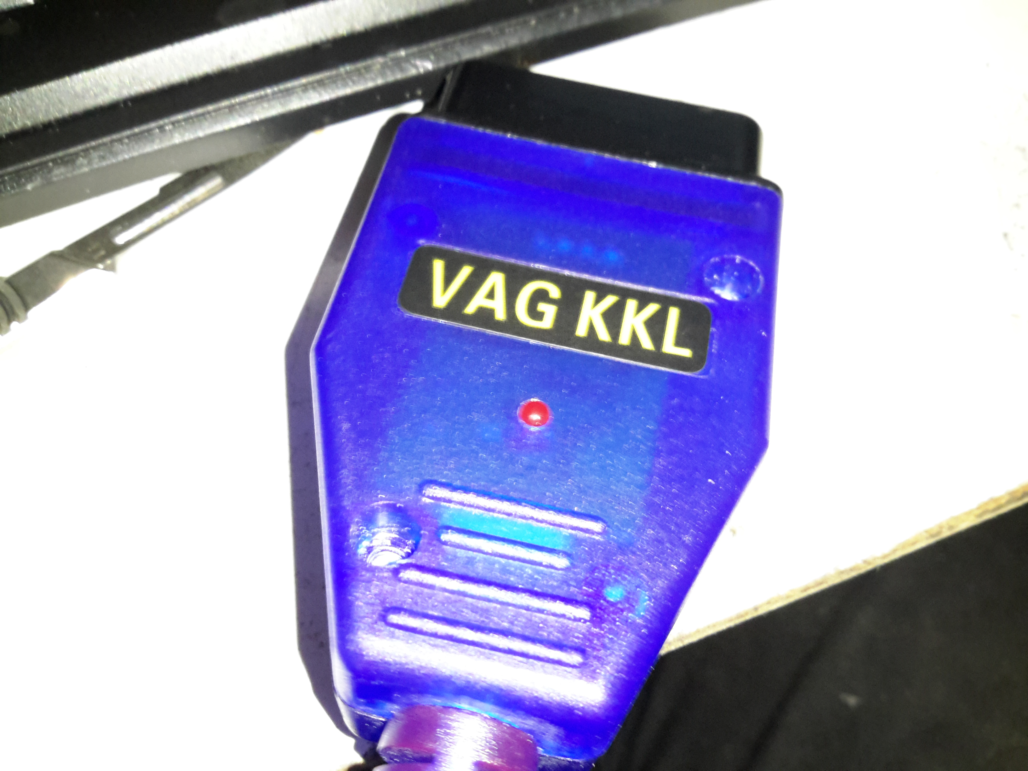
This is a little bit of kit I got to talk to the Webasto TT-V I salvaged from a scrap Jaguar S-Type, and converts USB-RS232 to the standard car diagnostic ODB connector. (These are a much cheaper option at £4 than the official Webasto diagnostic adaptor & loom which is over £90.
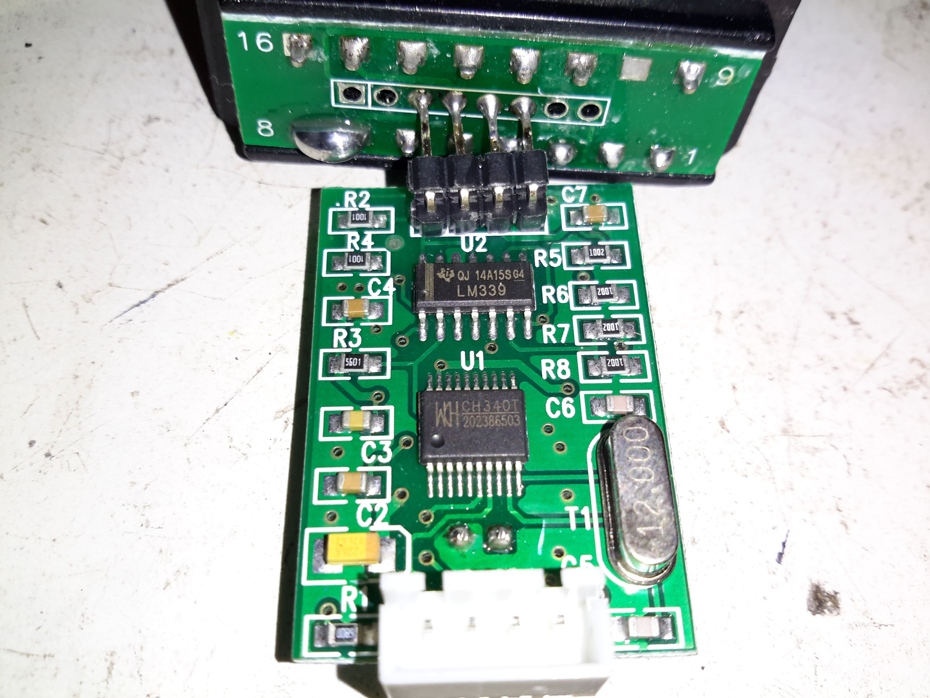
PCB Top
There’s really not much to this adaptor, the only signals that are routed to the ODB connector seem to be the +12v on pin 16, K-Line on Pin 7 & L-Line on pin 15. The main IC here is a CH340 USB-Serial interface, with some glue logic in the form of an LM339 quad comparator.
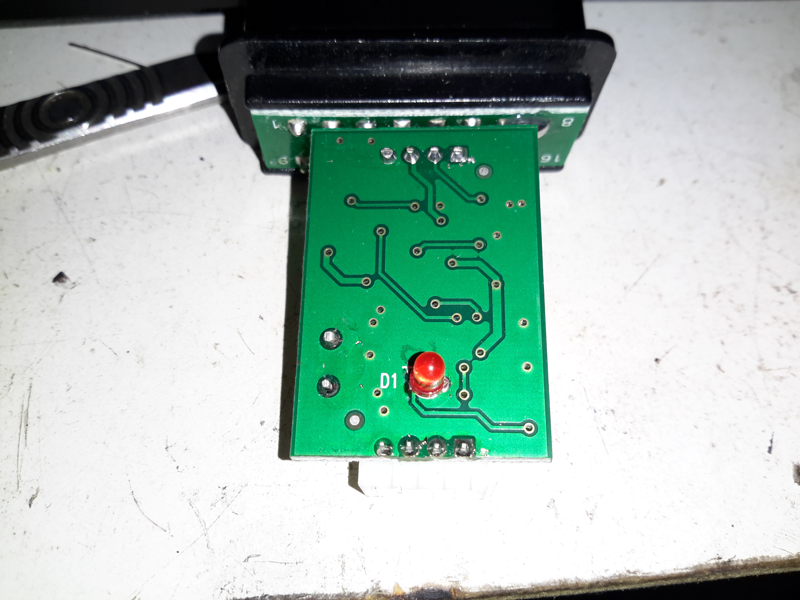
PCB Reverse
The reverse side of the PCB only has the power indicator LED.
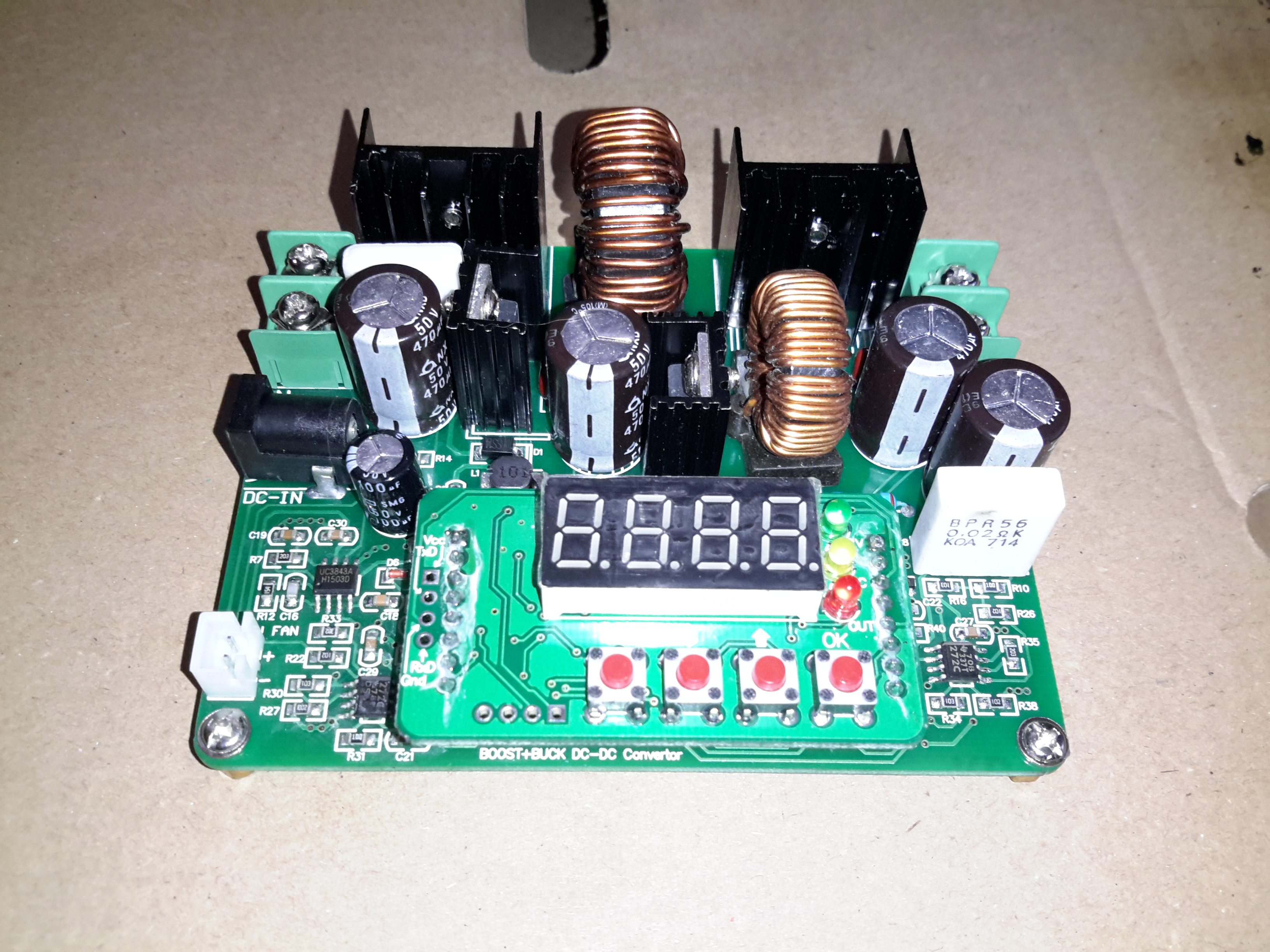
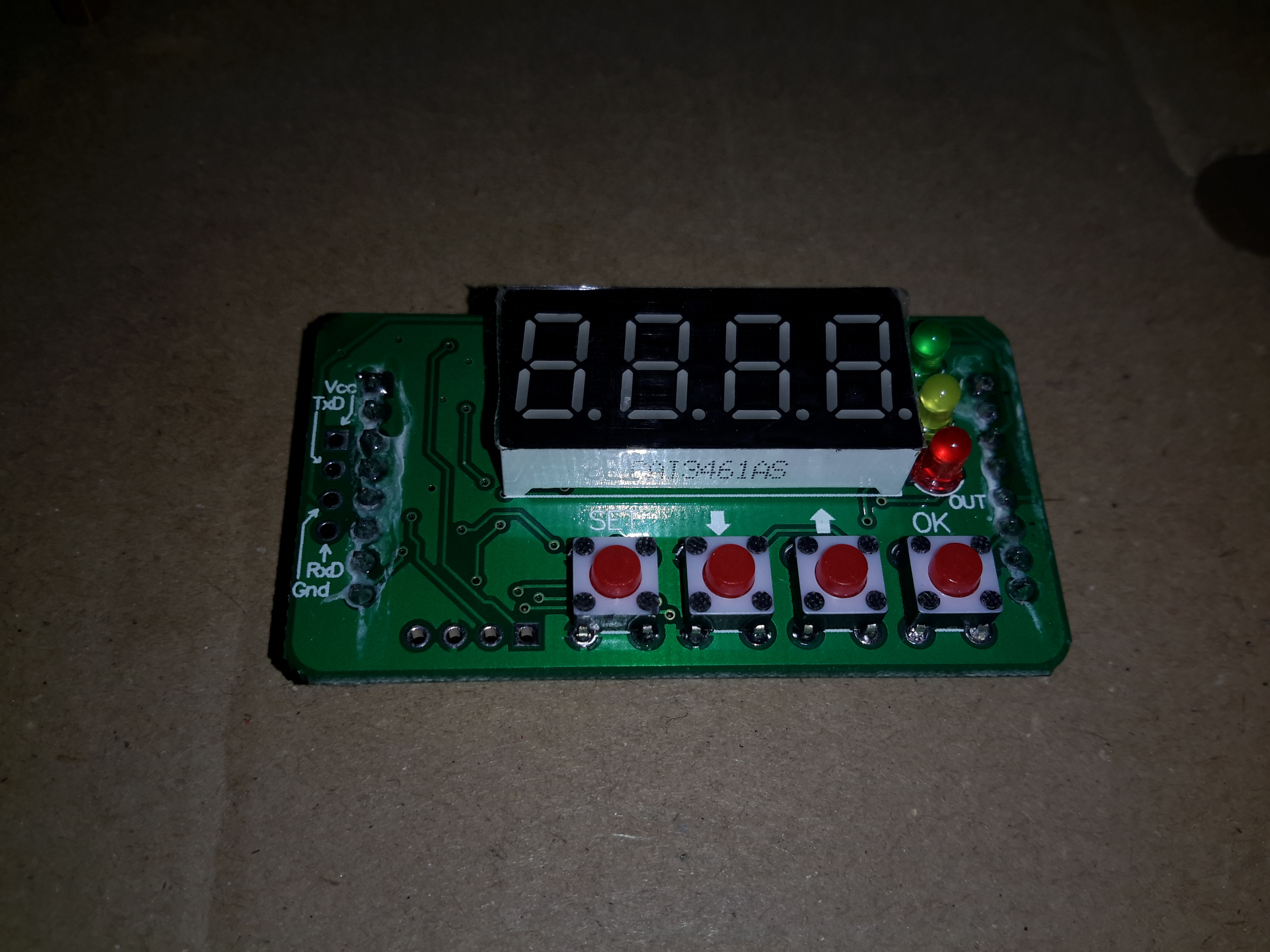
Here’s a useful buck-boost DC-DC converter from eBay, this one will do 36v DC at 6A maximum output current. Voltage & current are selected on the push buttons, when the output is enabled either the output voltage or the output current can be displayed in real time.
Display PCB
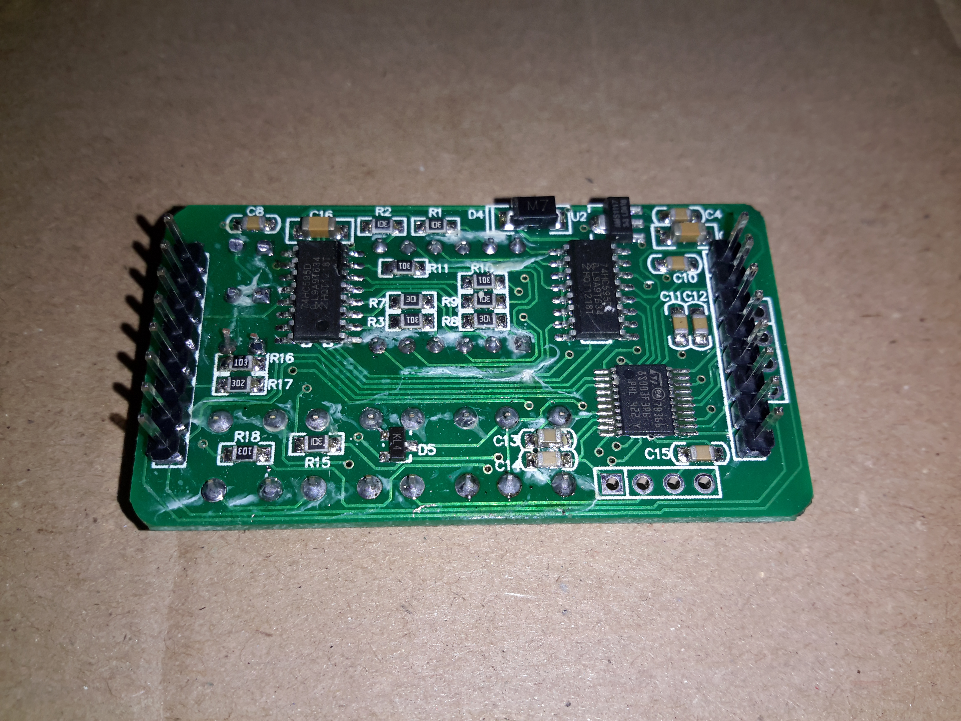
Here’s the display PCB, which also has the STM32 microcontroller that does all the magic. There appears to be a serial link on the left side, I’ve not yet managed to get round to hooking it into a serial adaptor to see if there’s anything useful on it.
Display Drive & Microcontroller
The bottom of the board holds the micro & the display multiplexing glue logic.
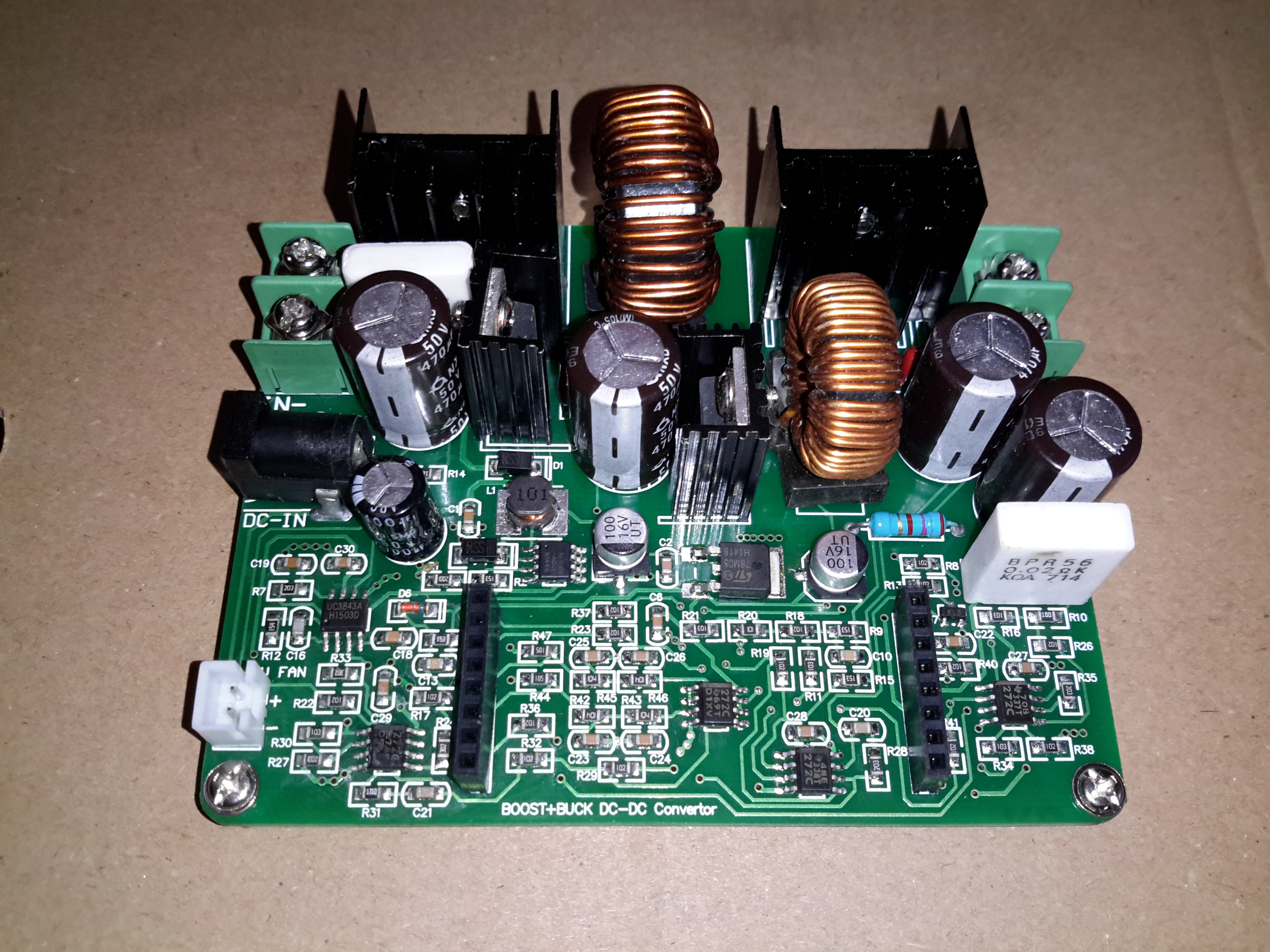
Main PCB
Not much on the mainboard apart from the large switching inductors & power devices. There’s also a SMPS PWM controller, probably being controlled from the micro.
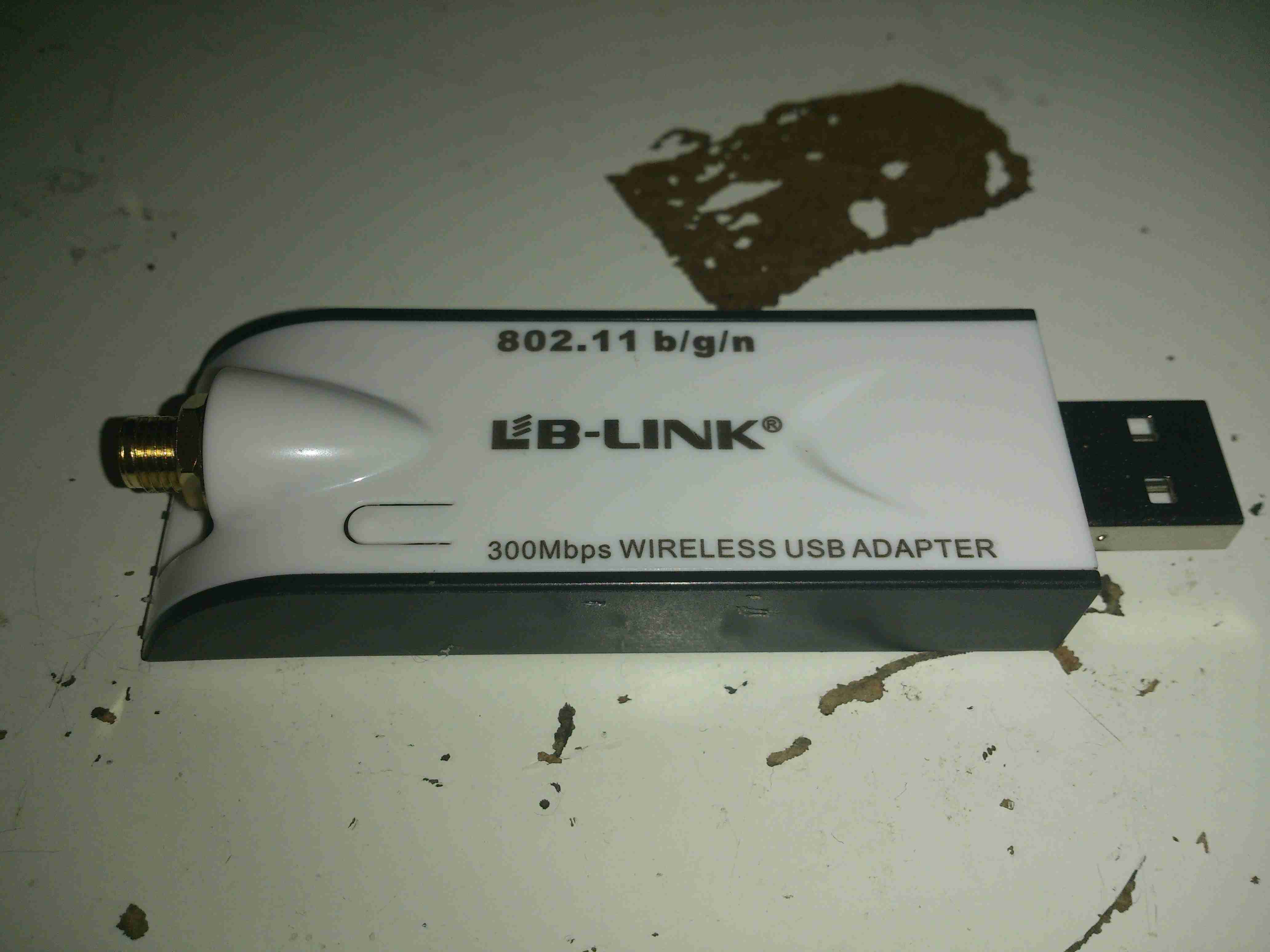
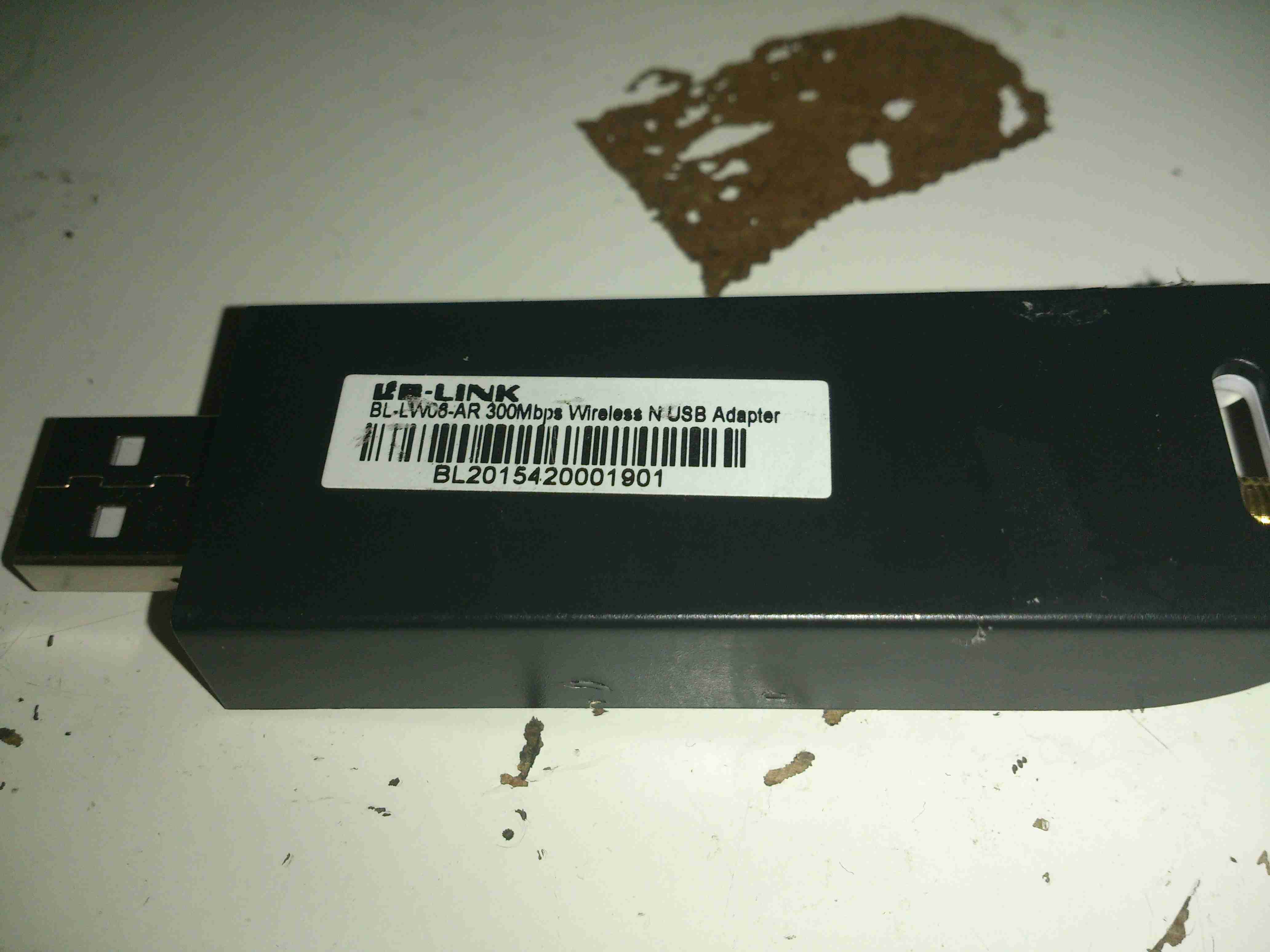
I needed a decent WiFi adaptor for my latest Pi LCD project, so after trawling eBay for cheapy USB adaptors, I found this one.
USB WiFi Dongle
Unlike most USB WiFi radios these days, it actually has a proper RP-SMA antenna connector, not the low-gain built in jobbies that never seem to work too well.
There are a few versions of this adaptor, all of which seem to use the same casing, there’s a button push cut into the plastic for a WPS button that doesn’t exist on this model. This is fine, as I don’t enable WPS on any of my network equipment anyway. (It’s insecure, and can be cracked in minutes).
MAC Address
Here’s the rest of the essential details, the model is BL-LW08-AR, rated at 300Mbit/s.
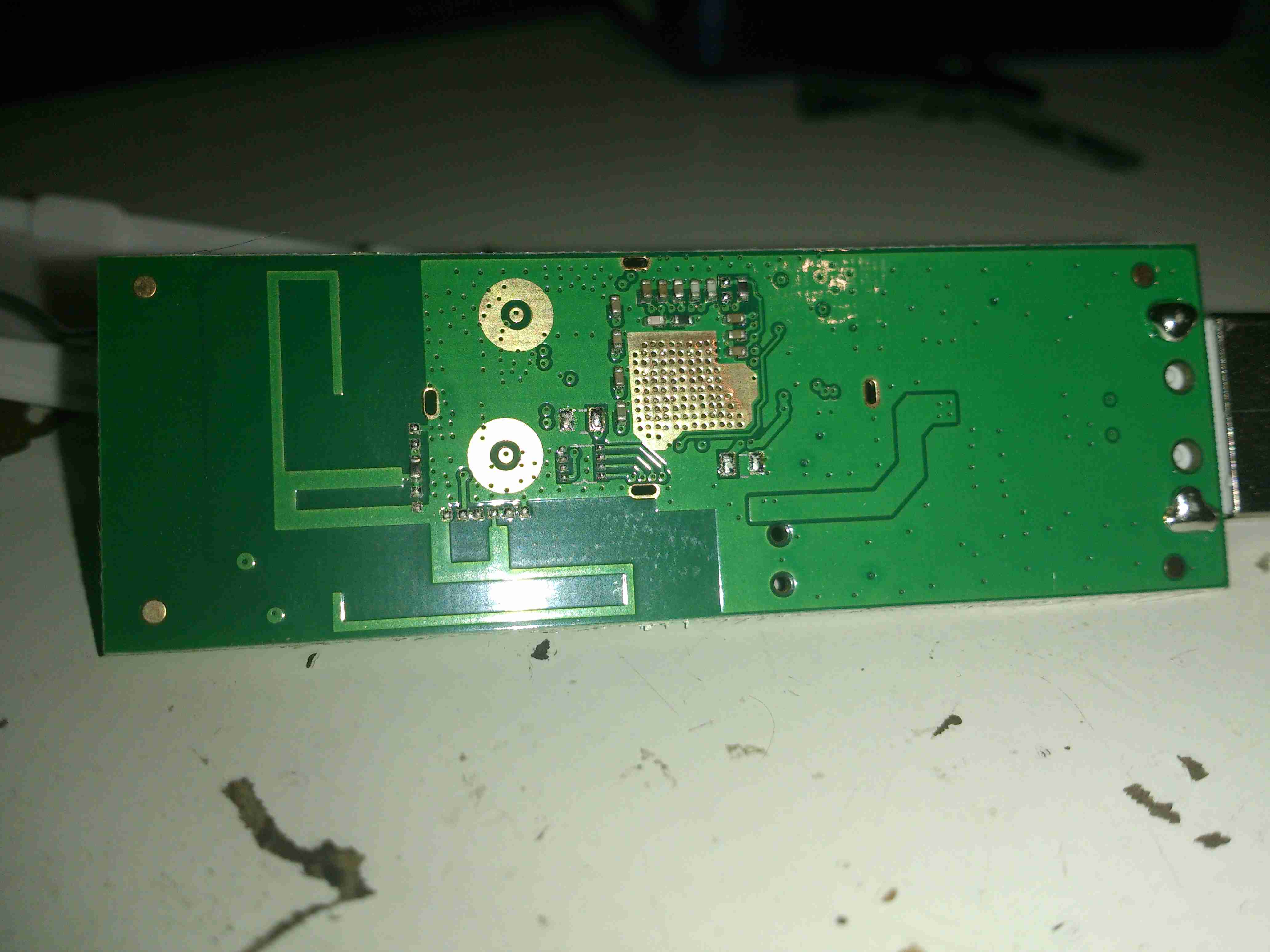
PCB Reverse
Here’s the PCB removed from the casing, there are a pair of PCB antennas on here, but they’re not connected to the RF circuitry in this model, the links are missing.
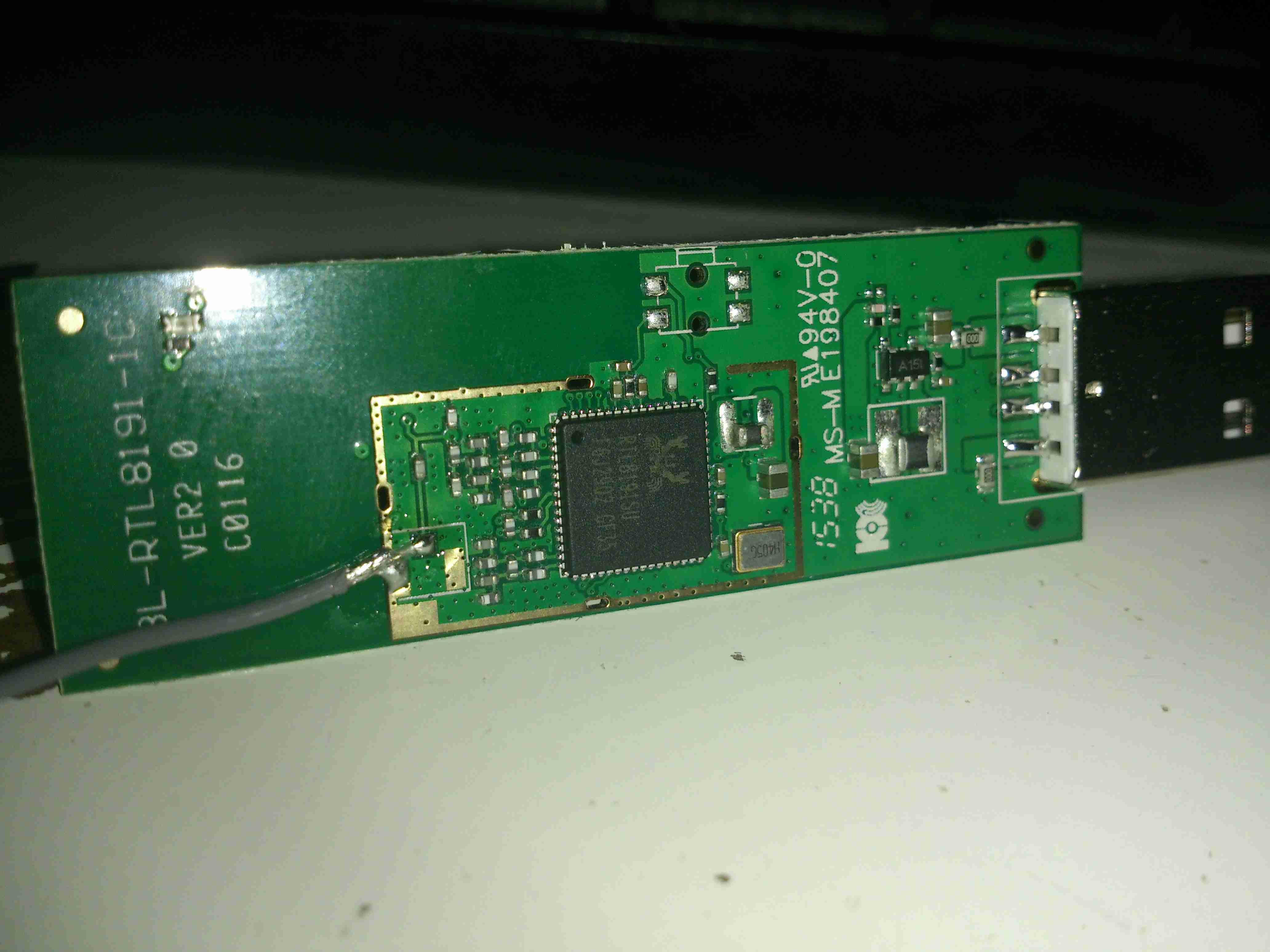
Chipset
The chipset used is a Realtek RTL8191SU, there isn’t much more in this device, as it’s all built into the silicon.
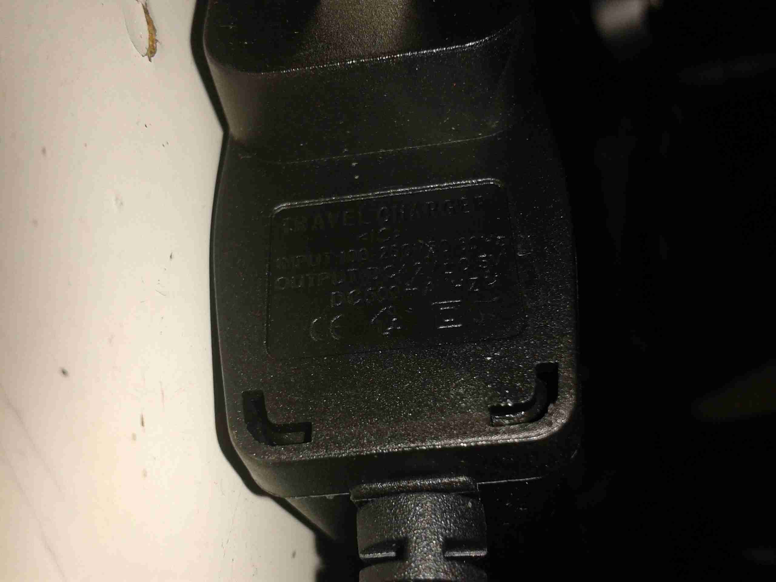
I almost forgot about this bit of kit, that came with one of my LED torches as a Lithium Ion charger. As I never plug in anything that comes from China via eBay, here’s the teardown & analysis.
Another Lethal Charger?
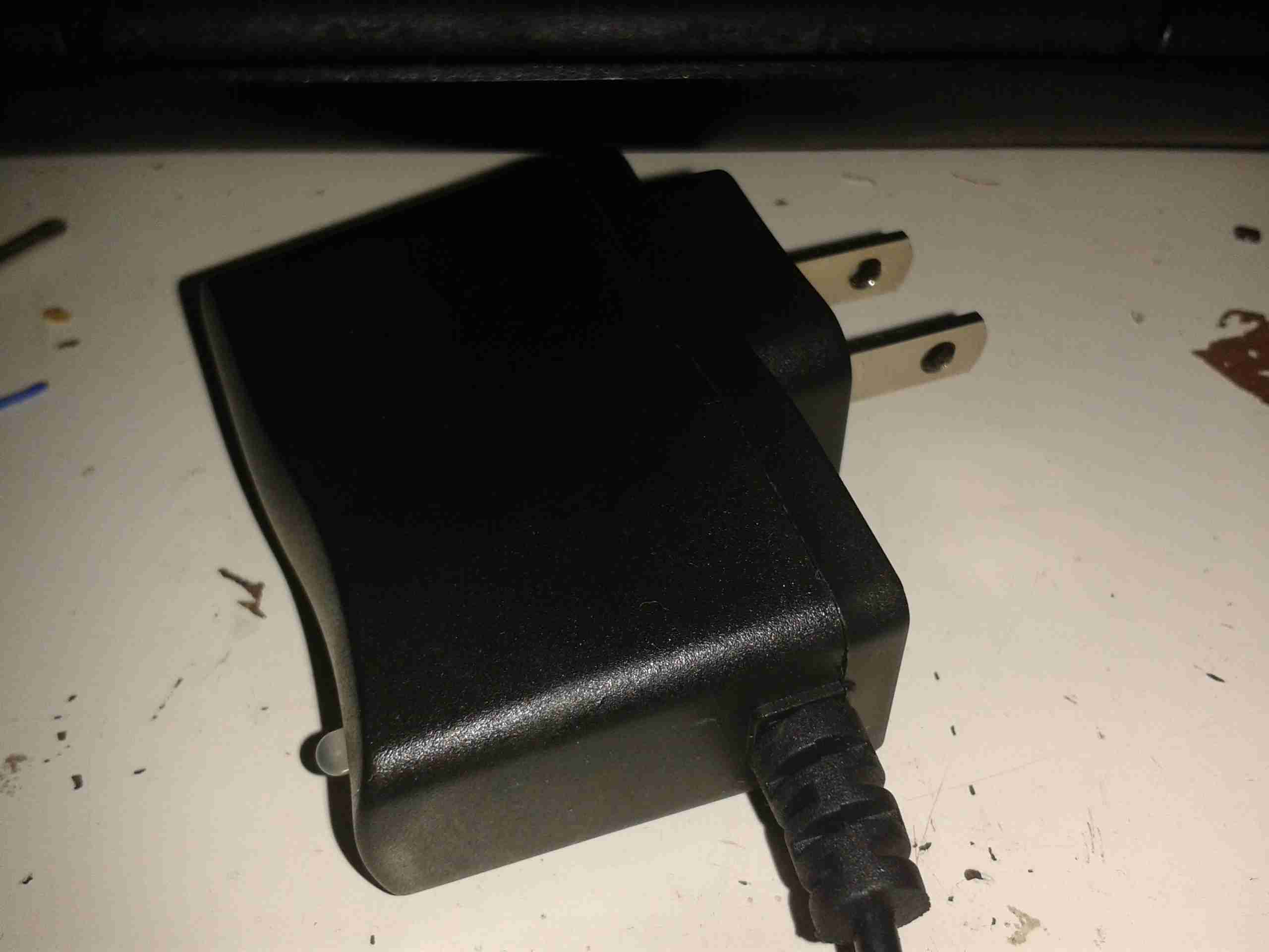
Here’s the unit itself. It’s very light, and is clearly intended for American NEMA power points.
Specs
Claimed specifications are 100-240v AC input, making it universal, and 4.2v DC out ±0.5v at 500mA.
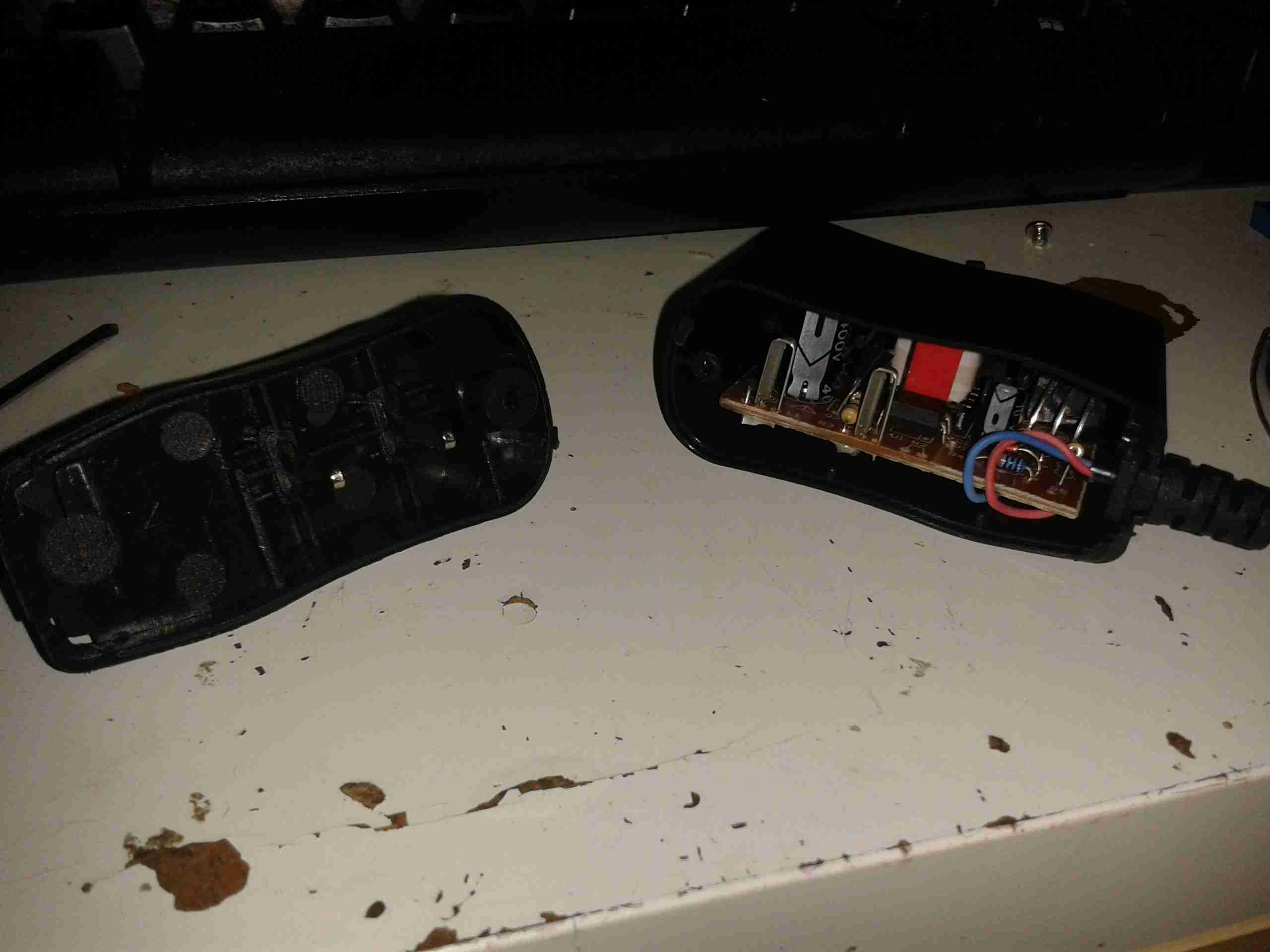
Considering the size of the output wire, if this can actually output rated voltage at rated current I’ll be surprised.
Opened
Here’s the adaptor opened up. There’s no mains wiring to speak of, the mains pins simply push into tags on the PCB.
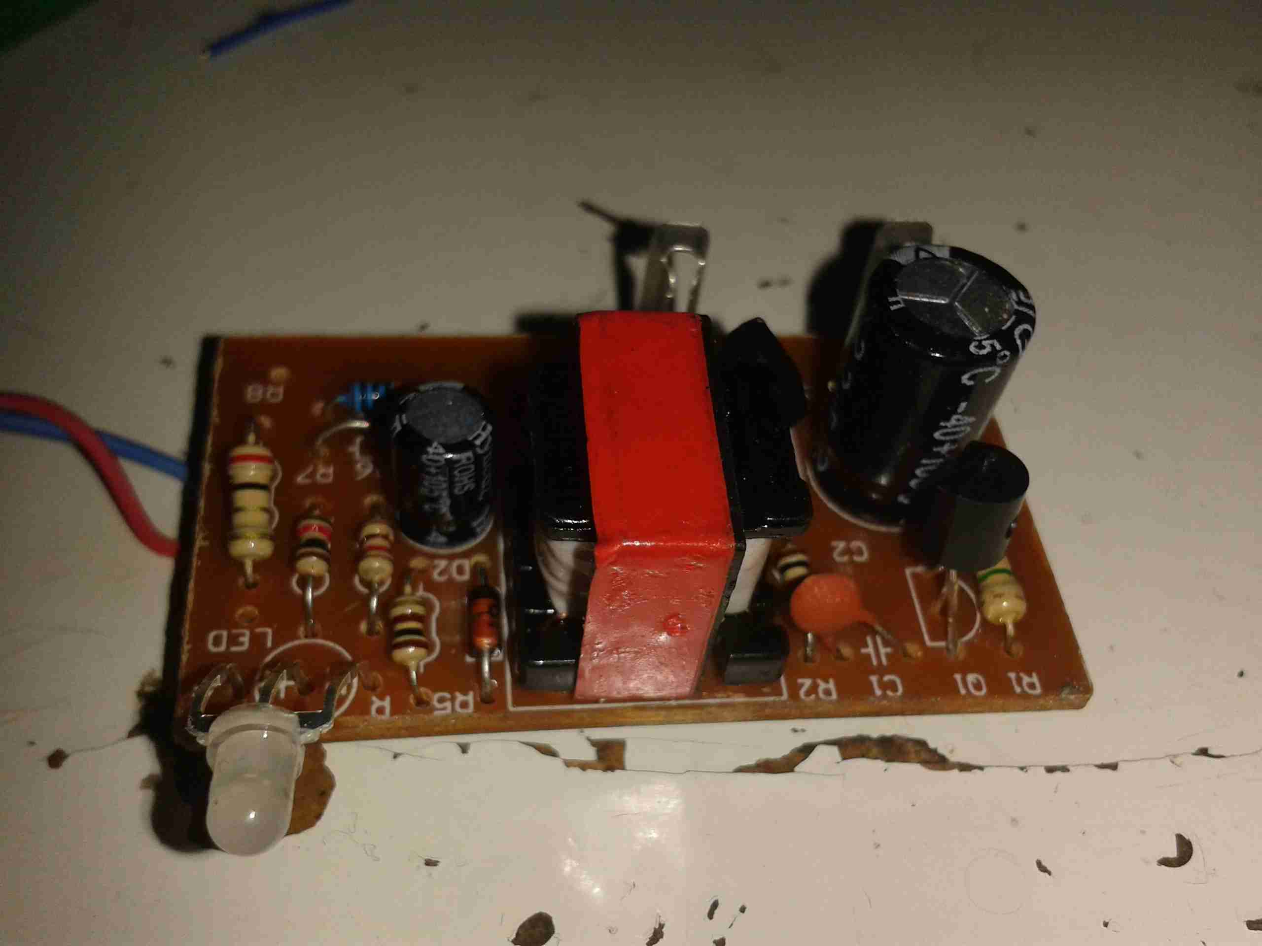
PCB Top
Top of the SMPS PCB. As usual with Chinese gear, it’s very simple, very cheap and likely very dangerous. There’s no real fusing on the mains input, only half-wave rectification & no EMI filtering.
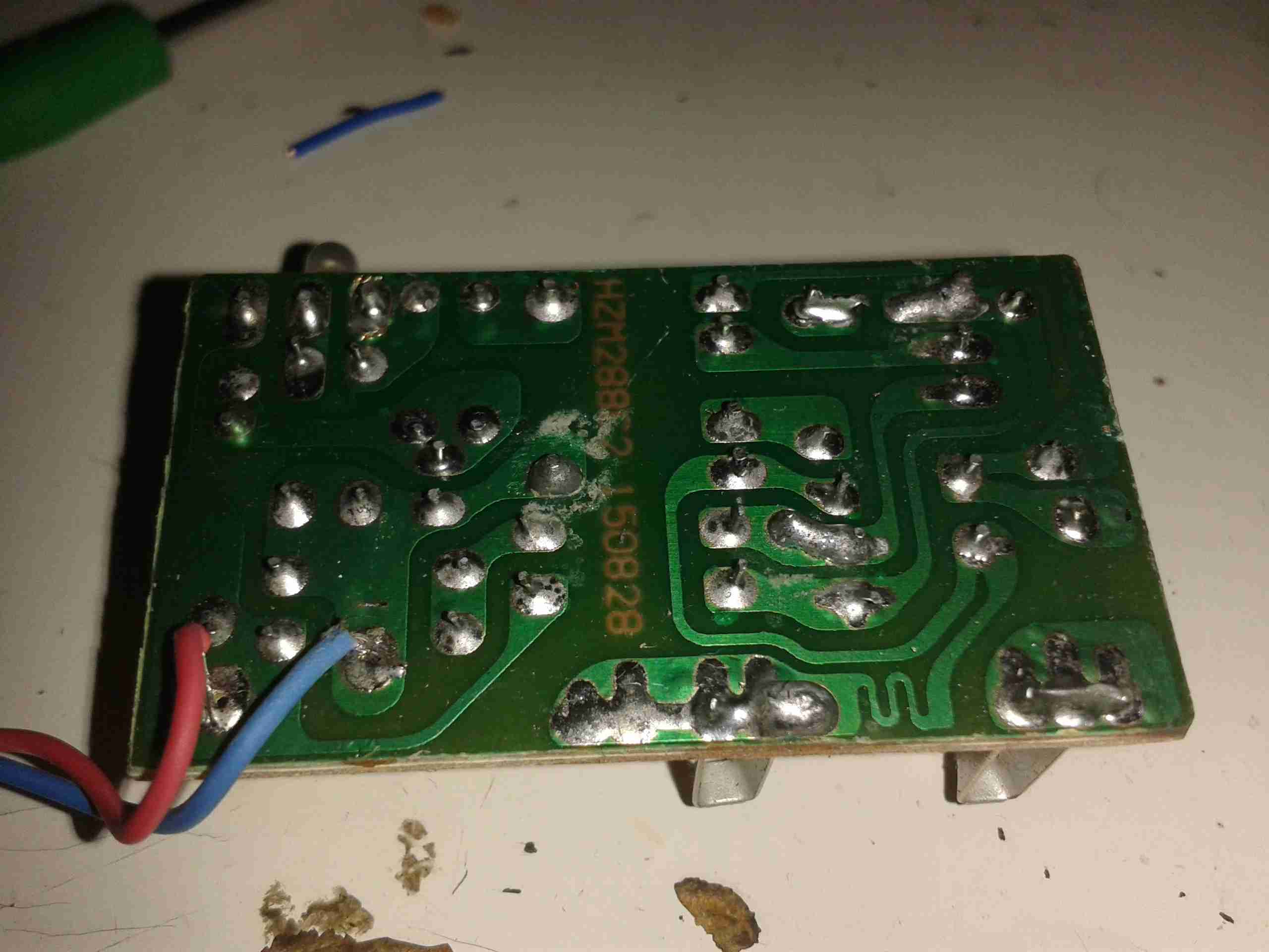
PCB Bottom
Here’s the bottom of the PCB. At least there’s a fairly sized gap between the mains & the output for isolation. The wiggly bit of track next to one of the mains input tags is supposed to be a fuse – I somehow doubt that it has the required breaking characteristics to actually pass any safety standards. Obviously a proper fuse or fusible resistor was far too expensive for these.
The output wiring on the left is thinner than hair, I’d say at least 28AWG, and probably can’t carry 500mA without suffering extreme volt drop.
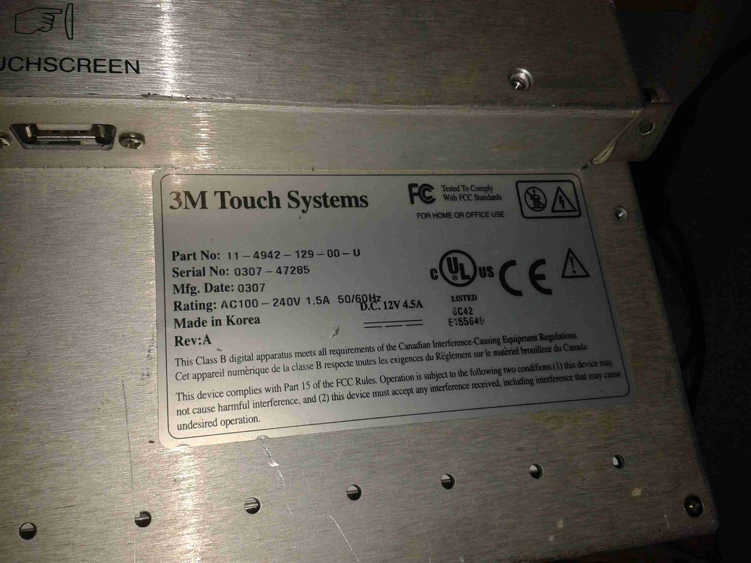
A while back I posted about a 3M Touch Systems industrial monitor that I’d been given. I had previously paired it with a Raspberry Pi Model B+, but for general desktop use it was just a little on the slow side.
Since the release of the Raspberry Pi 2, with it’s 4-core ARM Cortex CPU, things are much improved, so I figured I’d post an update with the latest on the system.
The monitor I’ve used is a commercial one, used in such things as POS terminals, service kiosks, etc. It’s a fairly old unit, but it’s built like a tank.
3M Panel
It’s built around a Samsung LTM170EI-A01 System-On-Panel, these are unusual in that all the control electronics & backlighting are built into the panel itself, instead of requiring an external converter board to take VGA to the required LVDS that LCD panels use for their interface.
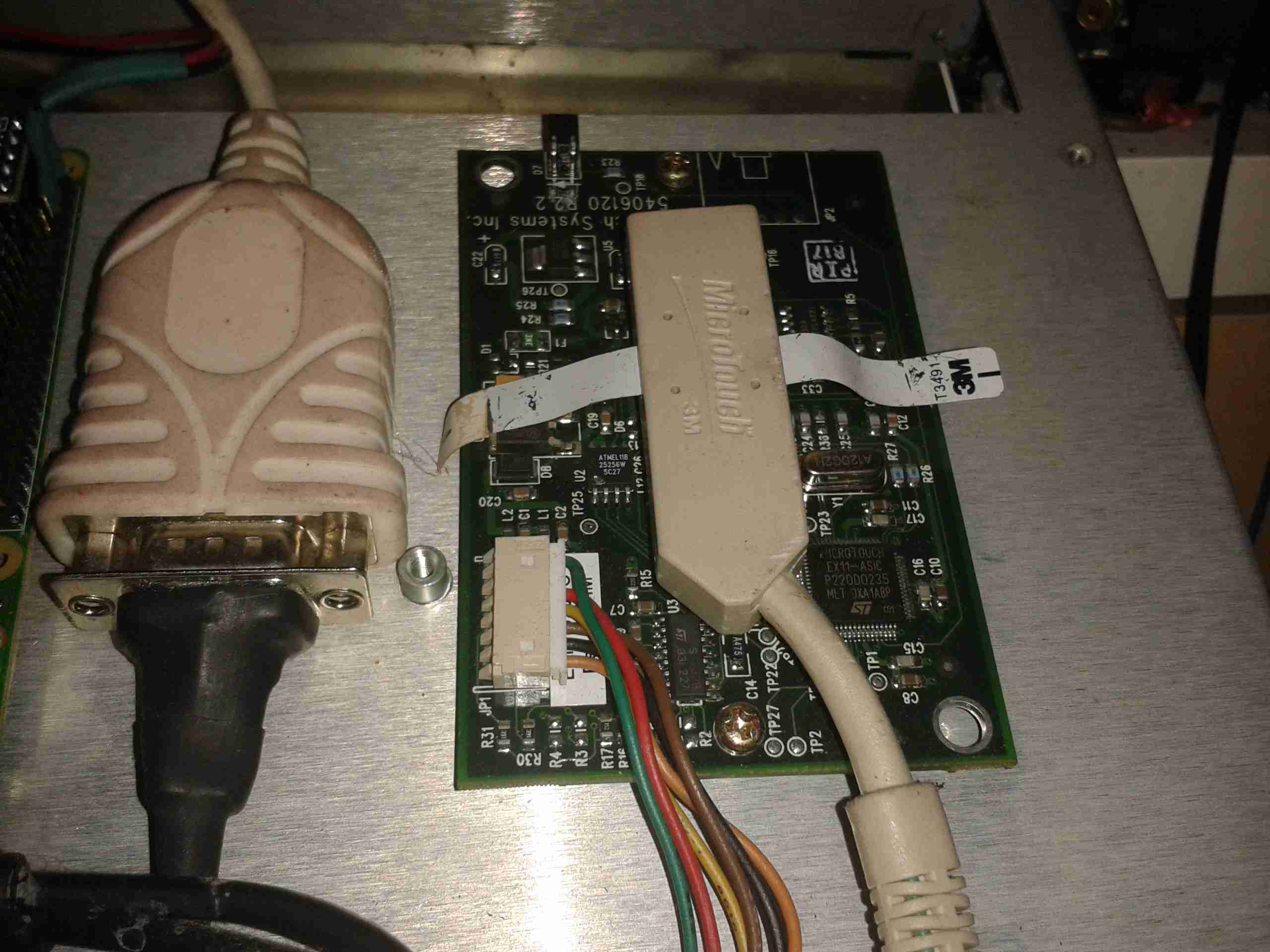
The touch section is a 3M Microtouch EXII series controller, with a surface capacitive touch overlay.
Touch Controller
Above is the touch controller PCB, with it’s USB-Serial converter to interface with the Pi.
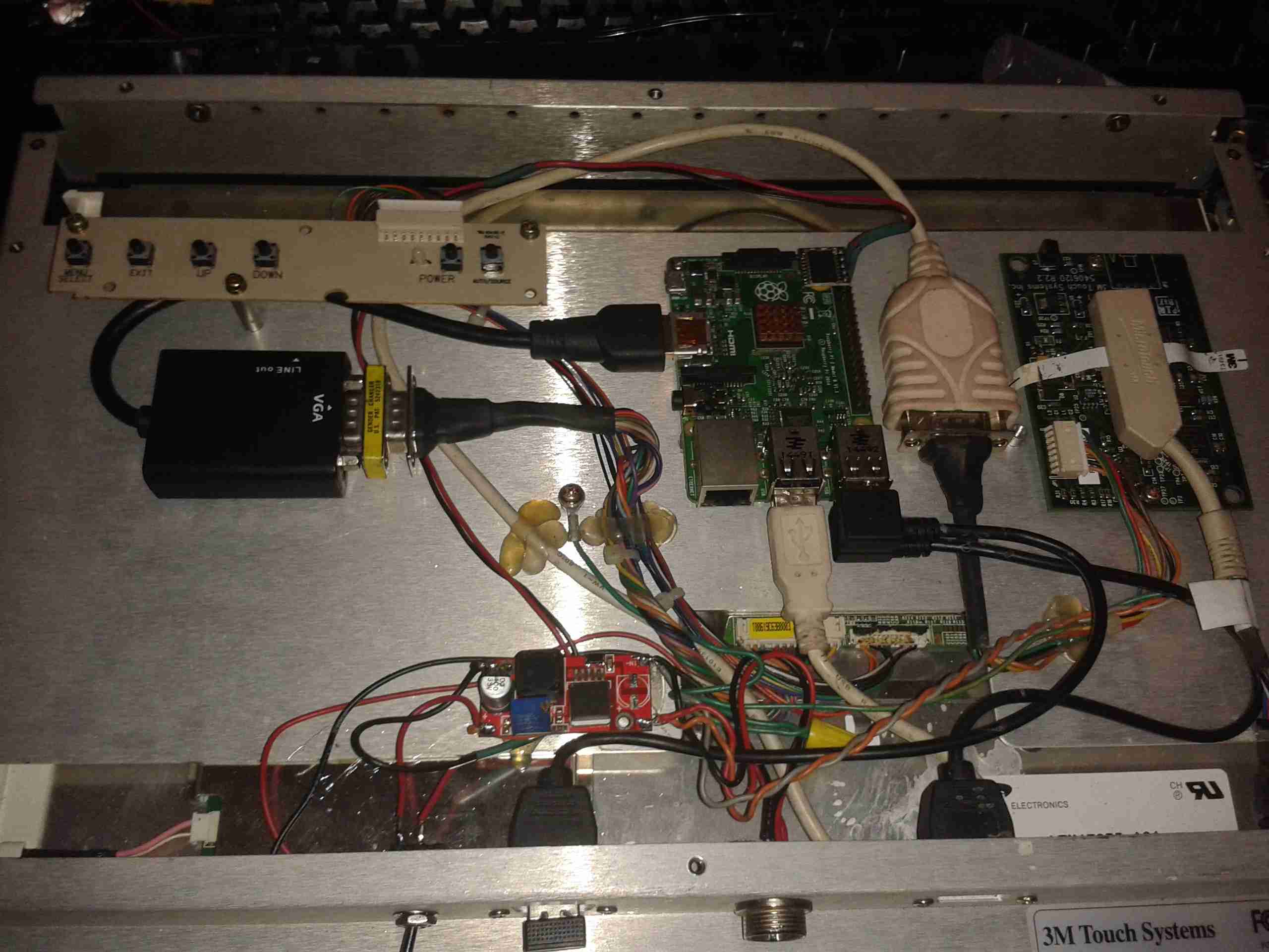
As there is much spare space inside the back of this monitor, I have mounted the Pi on a couple of spare screw posts, fitted USB ports where the original VGA & Serial connectors were in the casing, and added voltage regulation to provide the Pi with it’s required 5v.
Overview
Here’s the entire back of the panel, the Pi in the middle interfaces with a HDMI-VGA adaptor for the monitor, and the serial adaptor on the right for the touch. A small voltage regulator at the bottom of the unit is providing the 5v rail. There’s a switch at the bottom next to one of the USB ports to control power to the Pi itself. The panel won’t detect the resolution properly if they’re both powered on at the same time.
At 13.8v, the device pulls about 2A from the supply, which seems to be typical for a CCFL backlighted LCD.
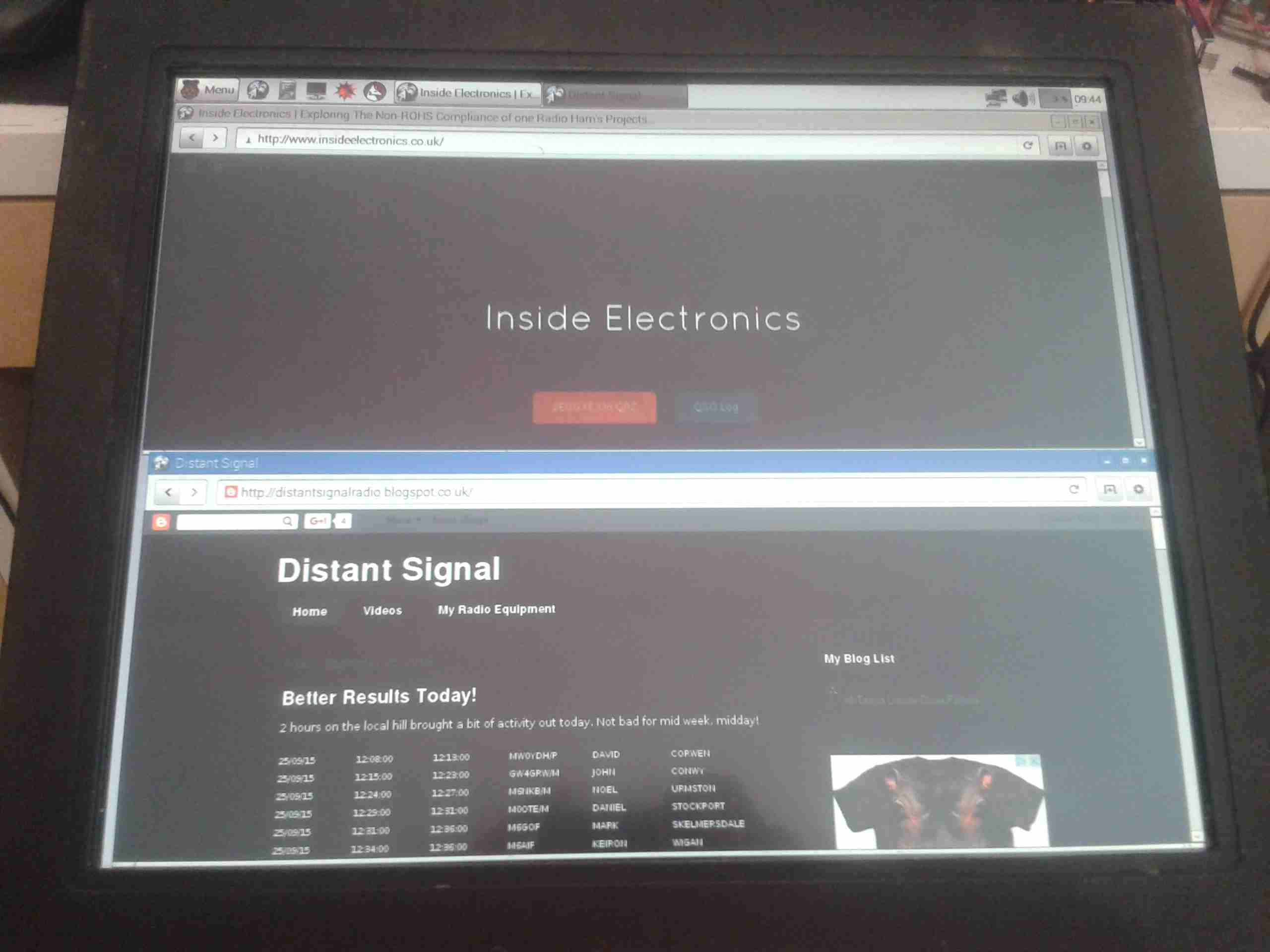
Now the Raspberry Pi 2 has been released, it’s much more responsive for desktop applications, especially with a slight overclock.
Shameless Plug
A full disk image enabled for Desktop & 3M touch monitors is available below for others that have similar panels. This image only works for the Pi 2!
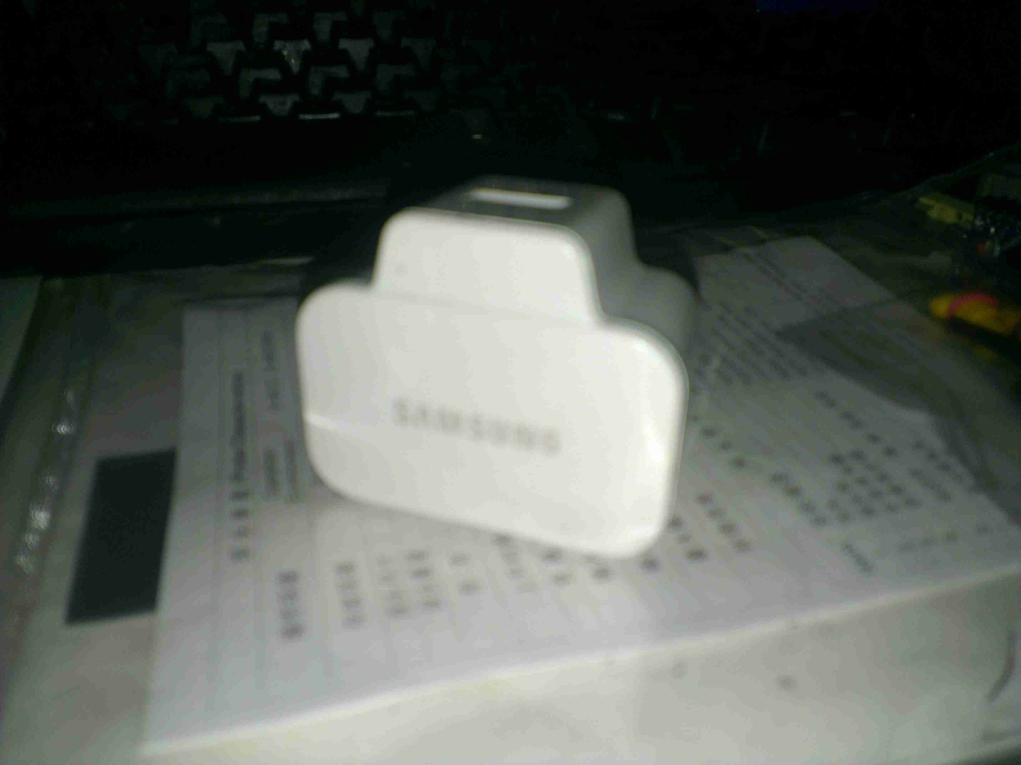
Here’s an odd & sudden failure, the power adaptor for a Samsung device. It’s been working for months & on being plugged into the mains today the magic blue smoke escaped.
Samsung Charger
It’s one of their 2A models, for charging bigger devices like tablets.
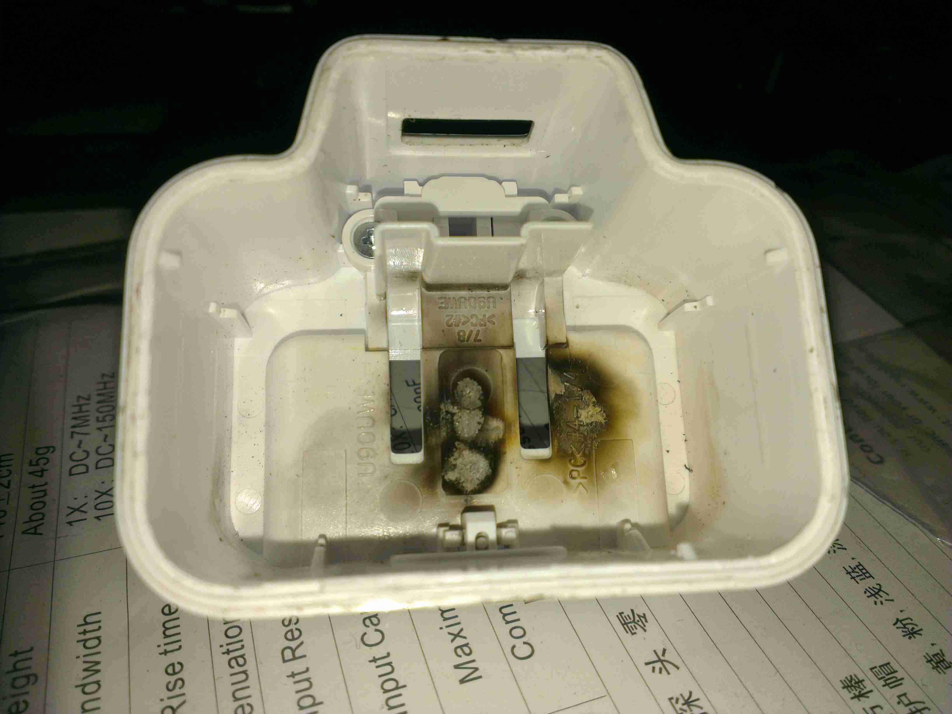
Flash Burn
Strangely for one of these chargers, no glue is used to hold it together – just clips. This made disassembly for inspection much easier. Evidence of a rather violent component failure is visible inside the back casing.
PCB
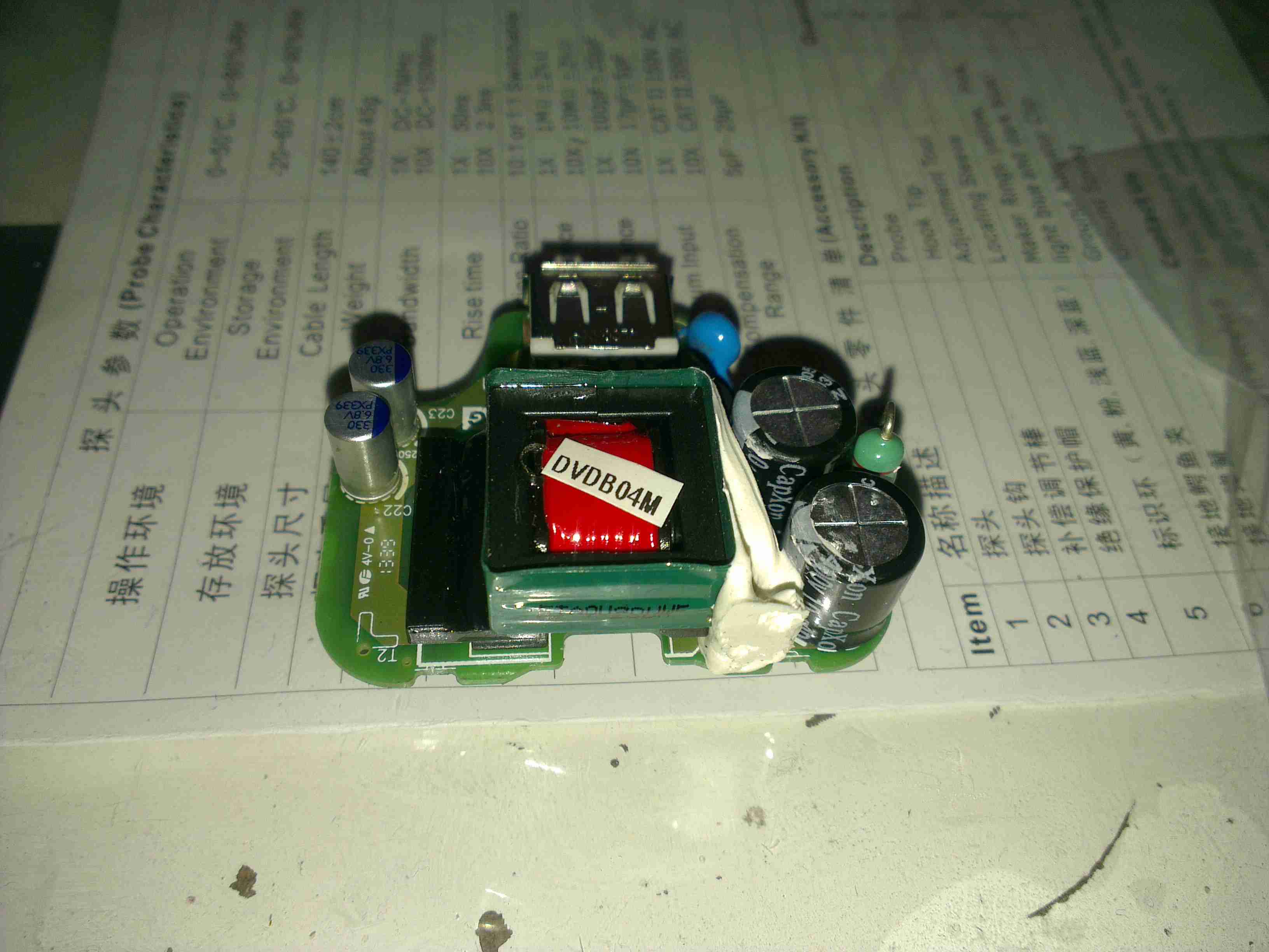
Here’s the charger PCB removed from the casing. As to be expected from Samsung, it’s a high quality unit, with all the features of a well designed SMPS.
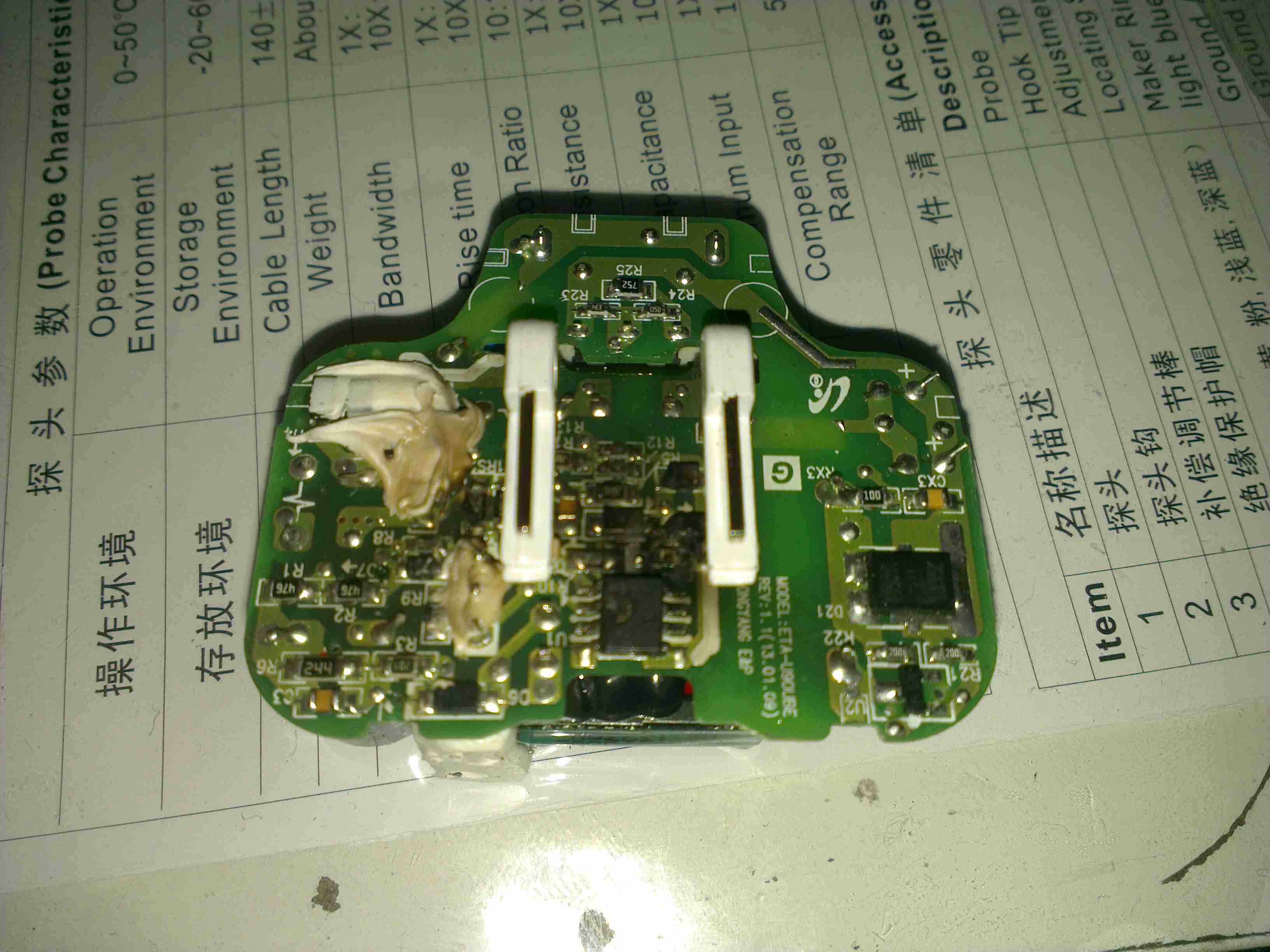
PCB Reverse
However, on turning the board over, the blown component is easily visible. It’s the main SMPS controller IC, with a massive hole blown in the top. The on board fuse has also blown open, but it obviously didn’t operate fast enough to save the circuit from further damage!
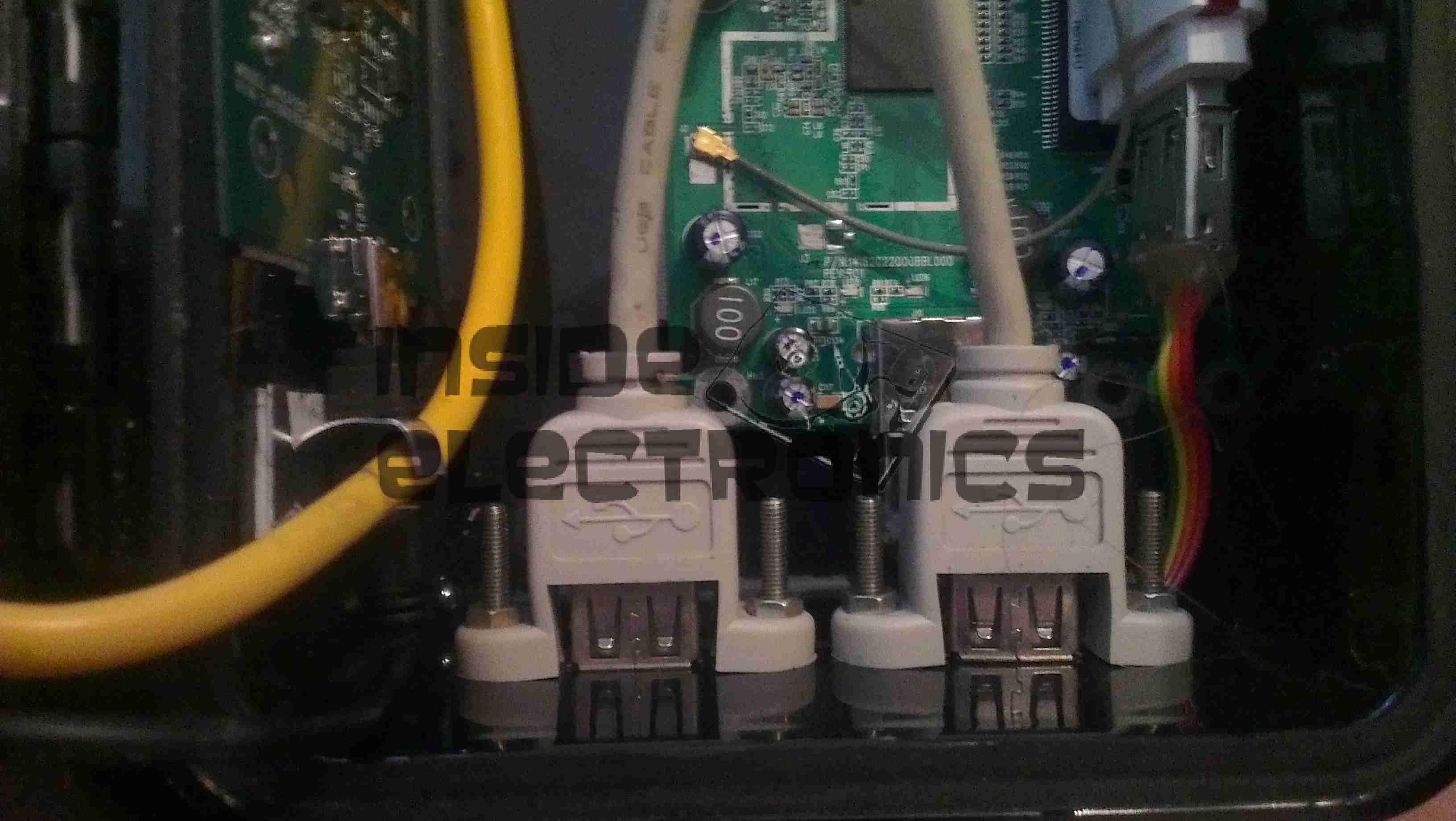
For convenience, a pair of USB ports have been fitted to the wearable Pi, which open on the bottom of the unit. These will be hardwired into a 4-port USB hub which will also support the wireless adaptor for the mini-keyboard that is to be used with the device.
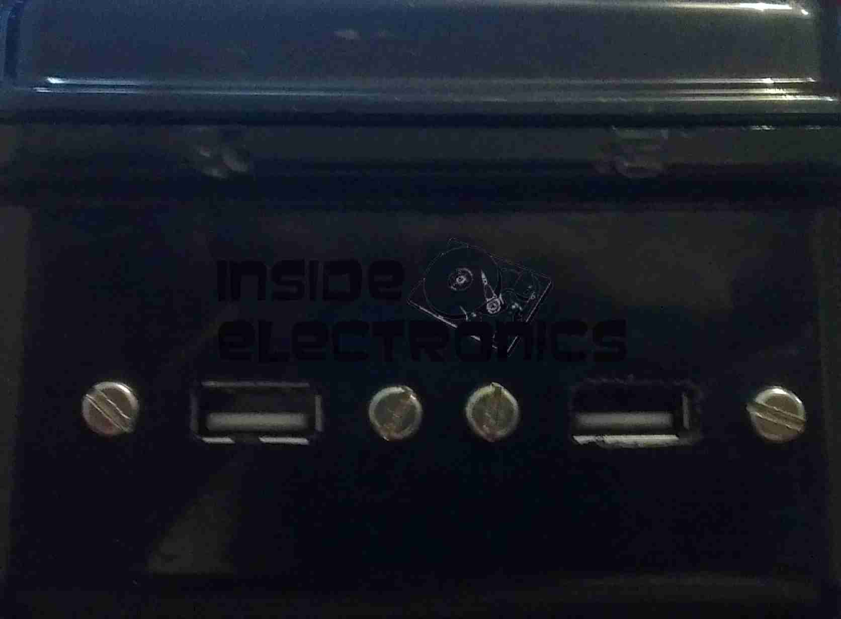
USBs
The two USB ports on the bottom of the casing.
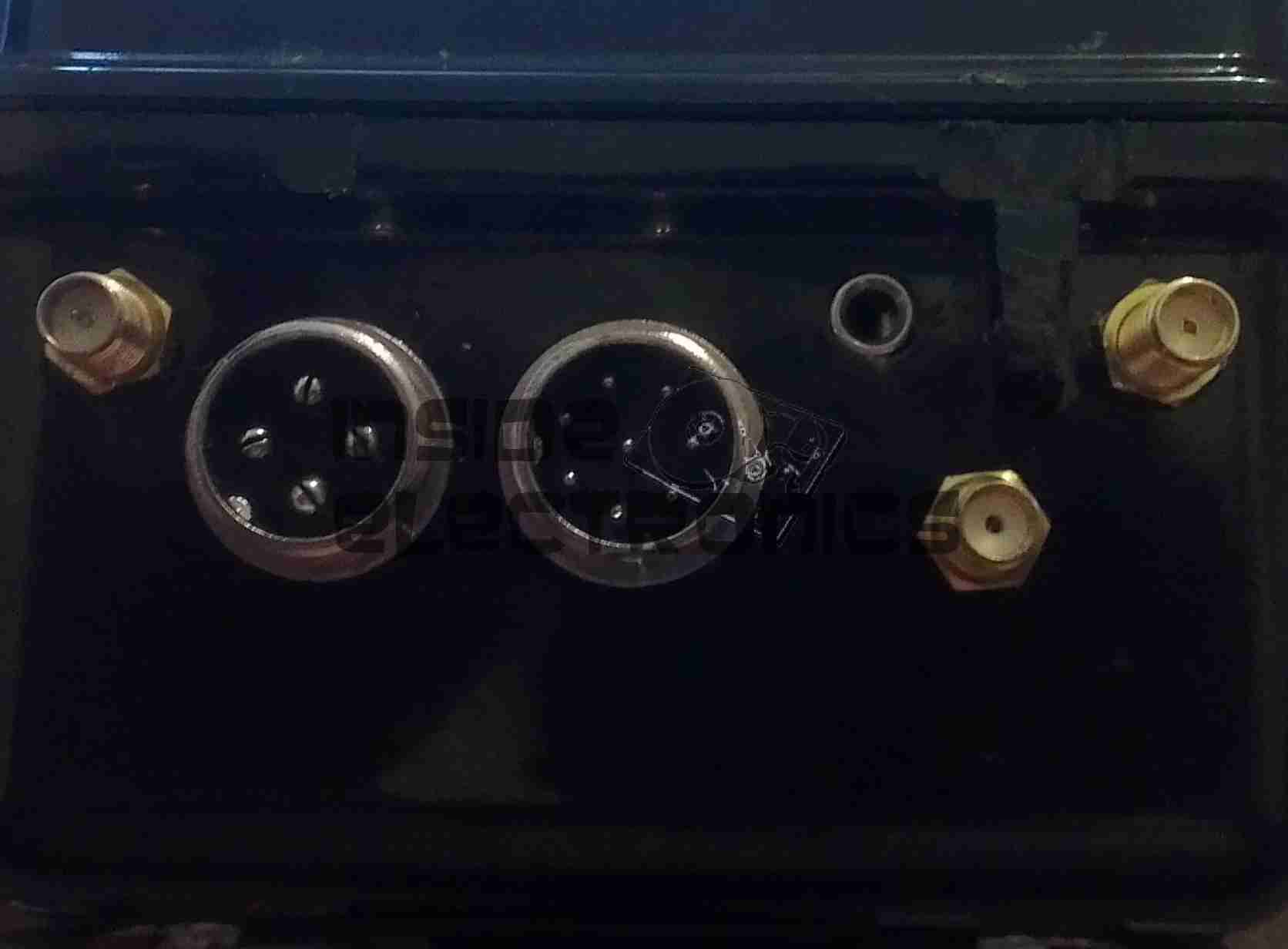
External Connections
The external connectors are also complete. The audio jack & second WiFi antenna port are fitted.
The audio is normally routed to the LCD display speaker, until a jack is plugged into the 3.5mm socket.
This is a device to use an IDE or SATA interface drive via a USB connection. Here is the front of the device, IDE interface at the bottom, 2.5″ form factor.
PCB Top
PCB removed from the casing. USB cable exits the top, 12v DC power jack to the left.
SATA interface below the DC Jack.
Molex connector below SATA is the power output for the drive in use. This unit has a built in 5v regulator.
PCB Bottom
Bottom of the PCB showing the interface IC.
Drive Adaptor
Adaptor to plug into the 44-pin 2.5″ form factor IDE interface on the adaptor, converts to standard 40-pin 3.5″ IDE.
Power Cable
Power pigtail with standard Molex & SATA power plugs.
This is an adaptor to convert computer VGA to composite & S-Video output for a normal TV.
Bottom
Bottom of the unit with option select switch.
PCB Top
PCB removed from the casing, CPU in centre, buffer RAM on the right.
PCB Bottom
Reverse side with the VGA connections at the top & the S-Video/composite outputs on the bottom.
VGA
Inputs. USB connector provides power, pair of VGA connectors provides passthrough function.
S-Video & Composite
Outputs. Standard S-Video on the left & composite video on the right.
Tip Jar
If you’ve found my content useful, please consider leaving a donation by clicking the Tip Jar below!
All collected funds go towards new content & the costs of keeping the server online.