Time for another teardown! I managed to fish this Sky+ box out of a skip, but to protect the guilty, all serial numbers have been removed.
These are pretty smart devices, with DVR capability on board.
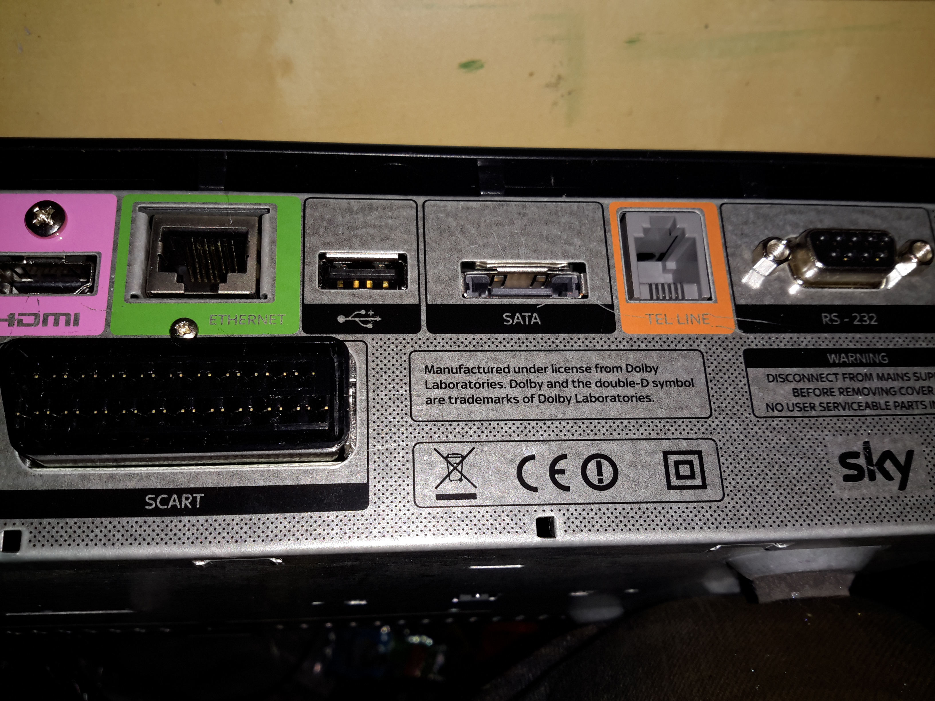
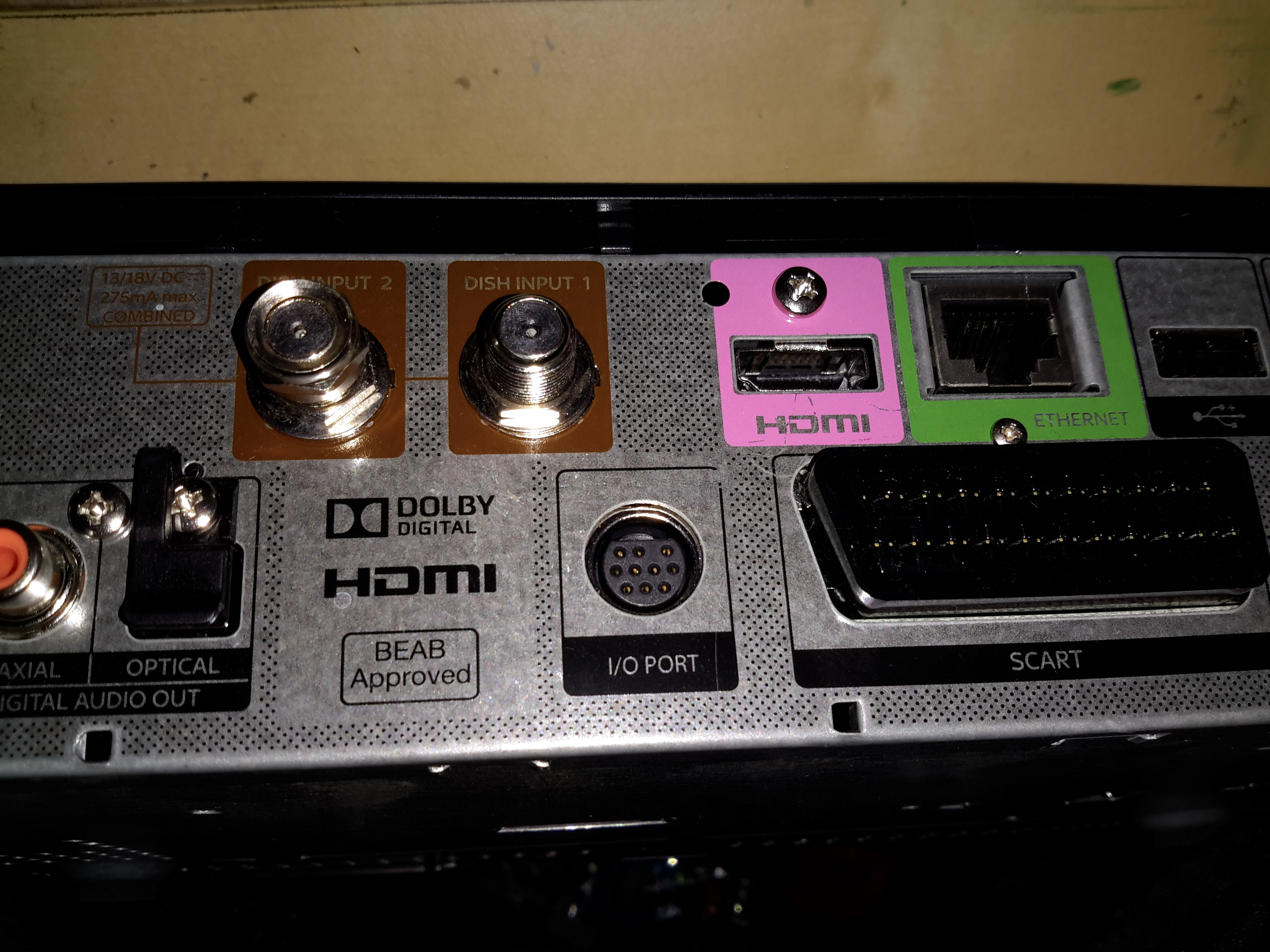
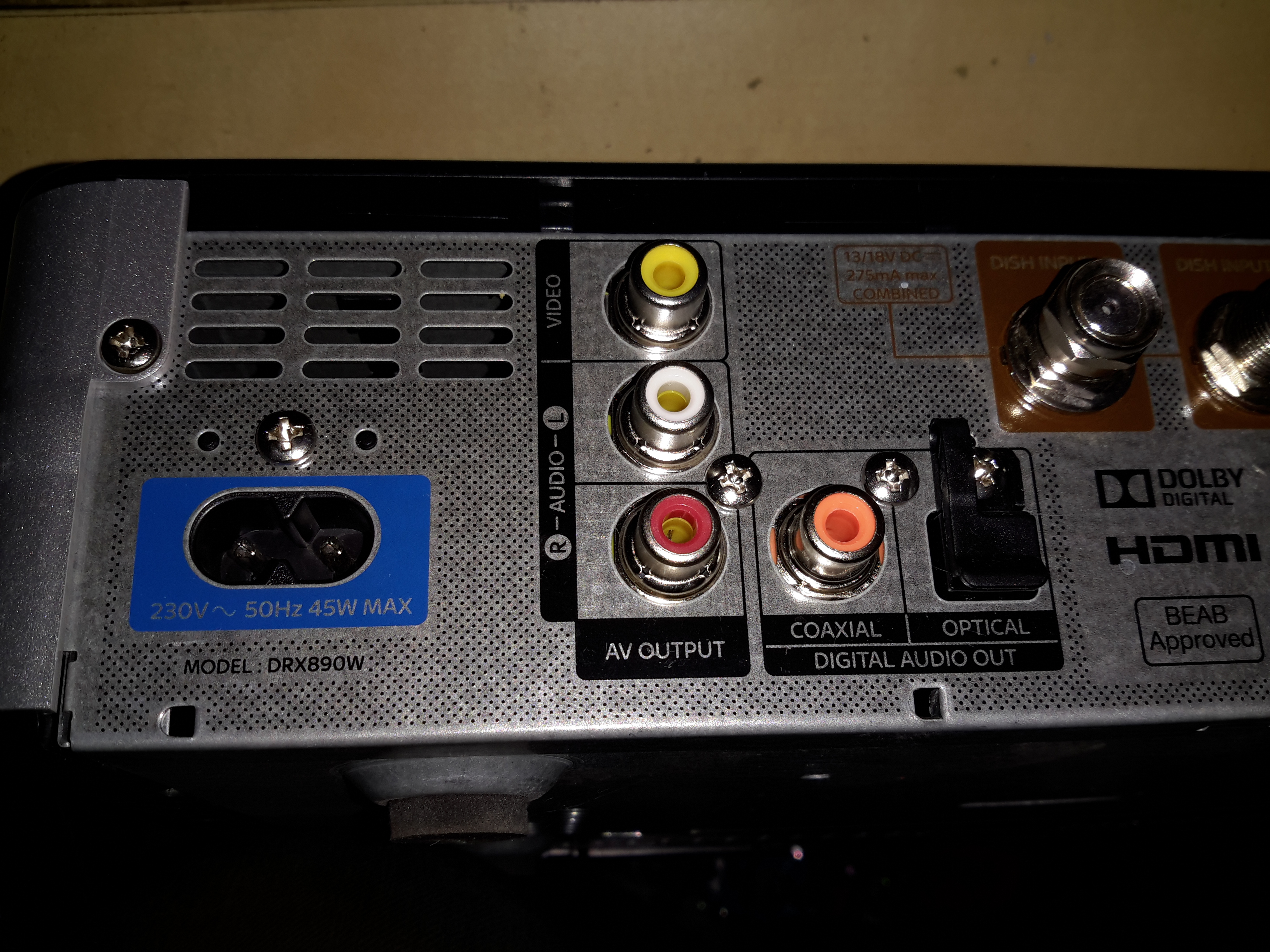
Ports 1
There’s a lot of ports on these units, from RS-232 serial, POTS modem, eSATA, HDMI, USB, Ethernet, SCART, Optical, digital outputs & even composite video.
Ports 2Ports 3Top Panel
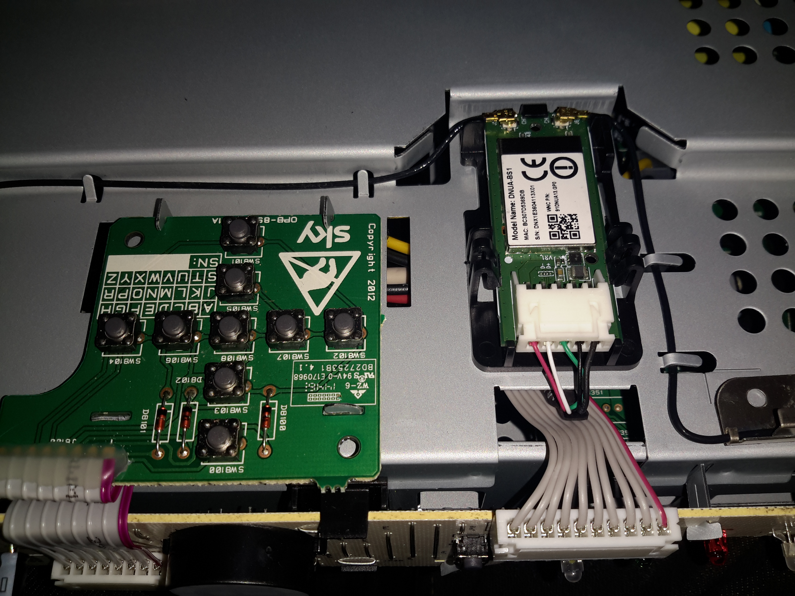
Removing the top plastic cover reveals the operation buttons & the built in WiFi adaptor, which is USB connected to the main logic board.
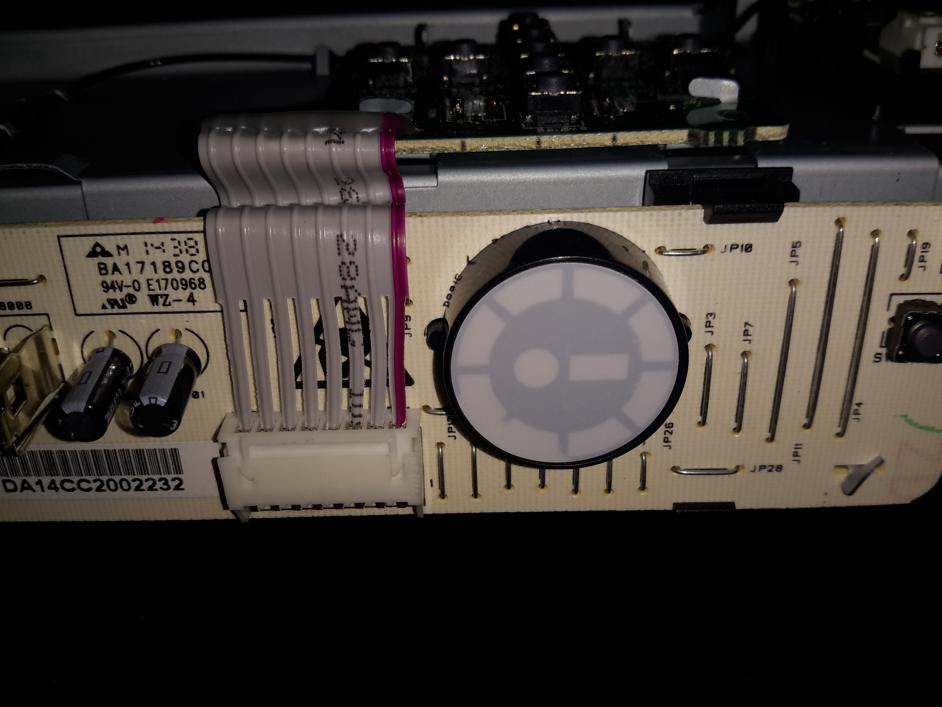
Front Panel
The PCB on the front of the chassis has all the indicators, and the IR Receiver for the remote.
Cover Removed
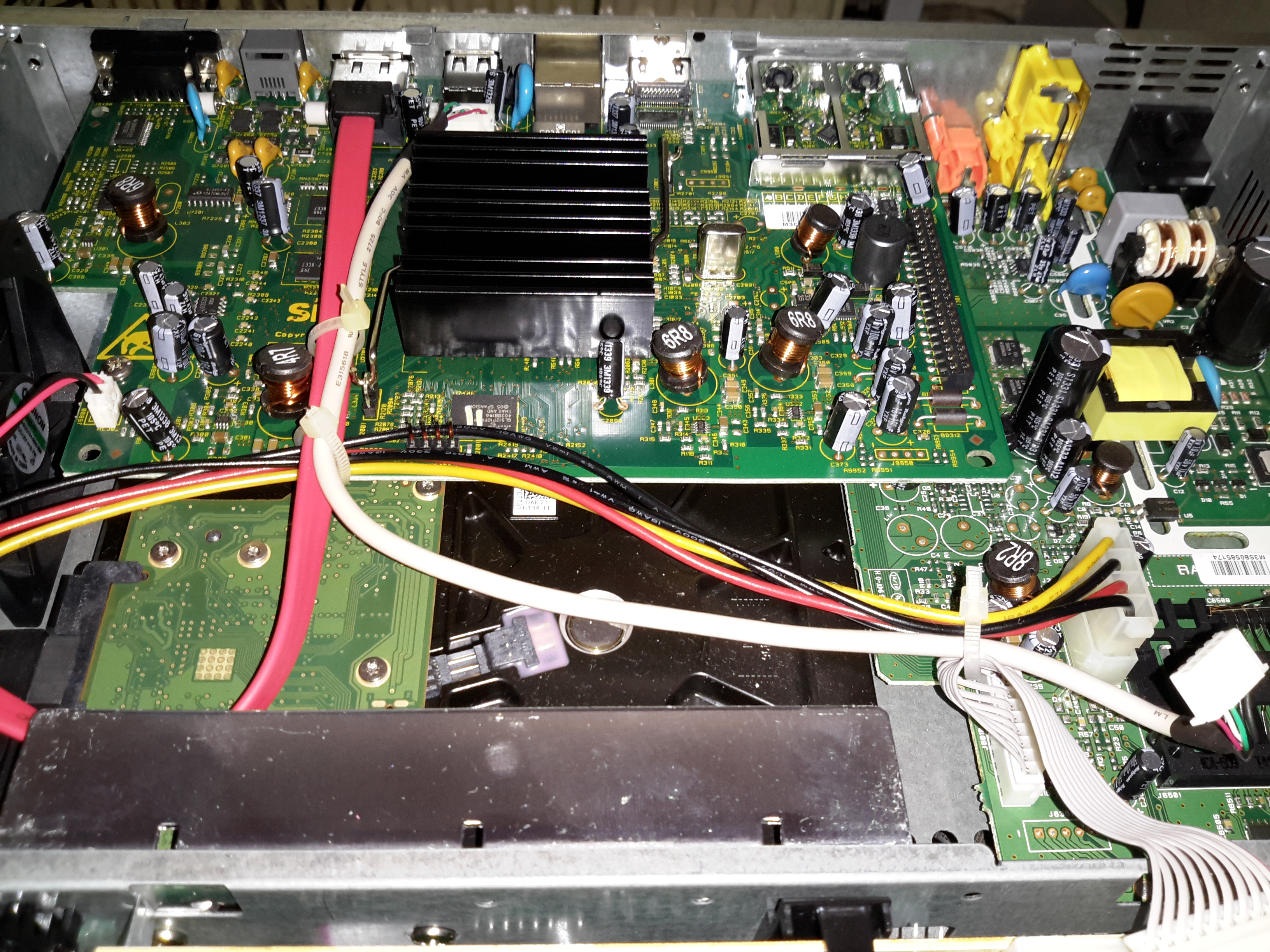
Removing the top shield of the chassis reveals the innards. The PSU is on the top right, 500GB SATA disk drive in the bottom centre. The main logic PCB is top centre.
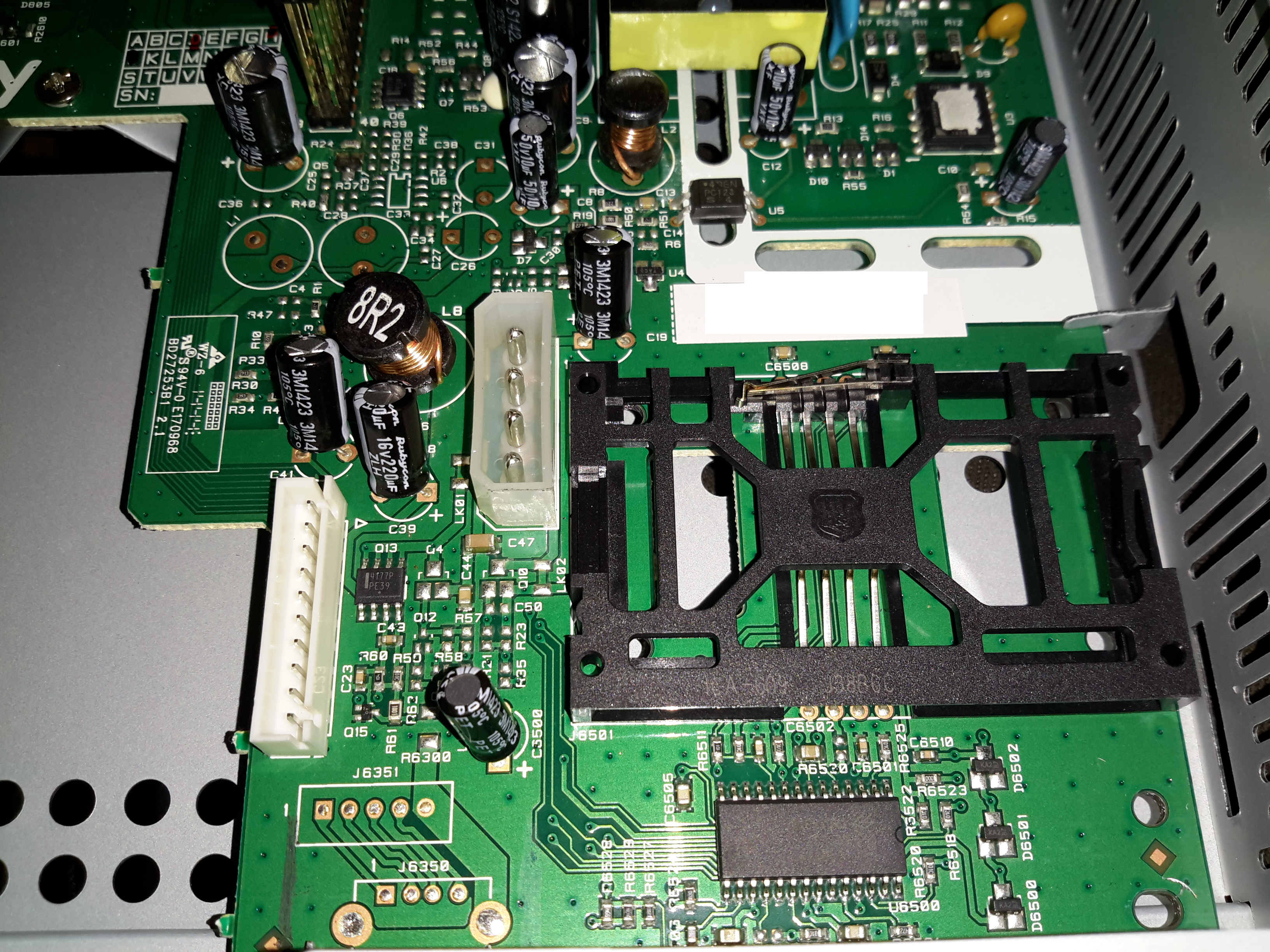
Logic PCB
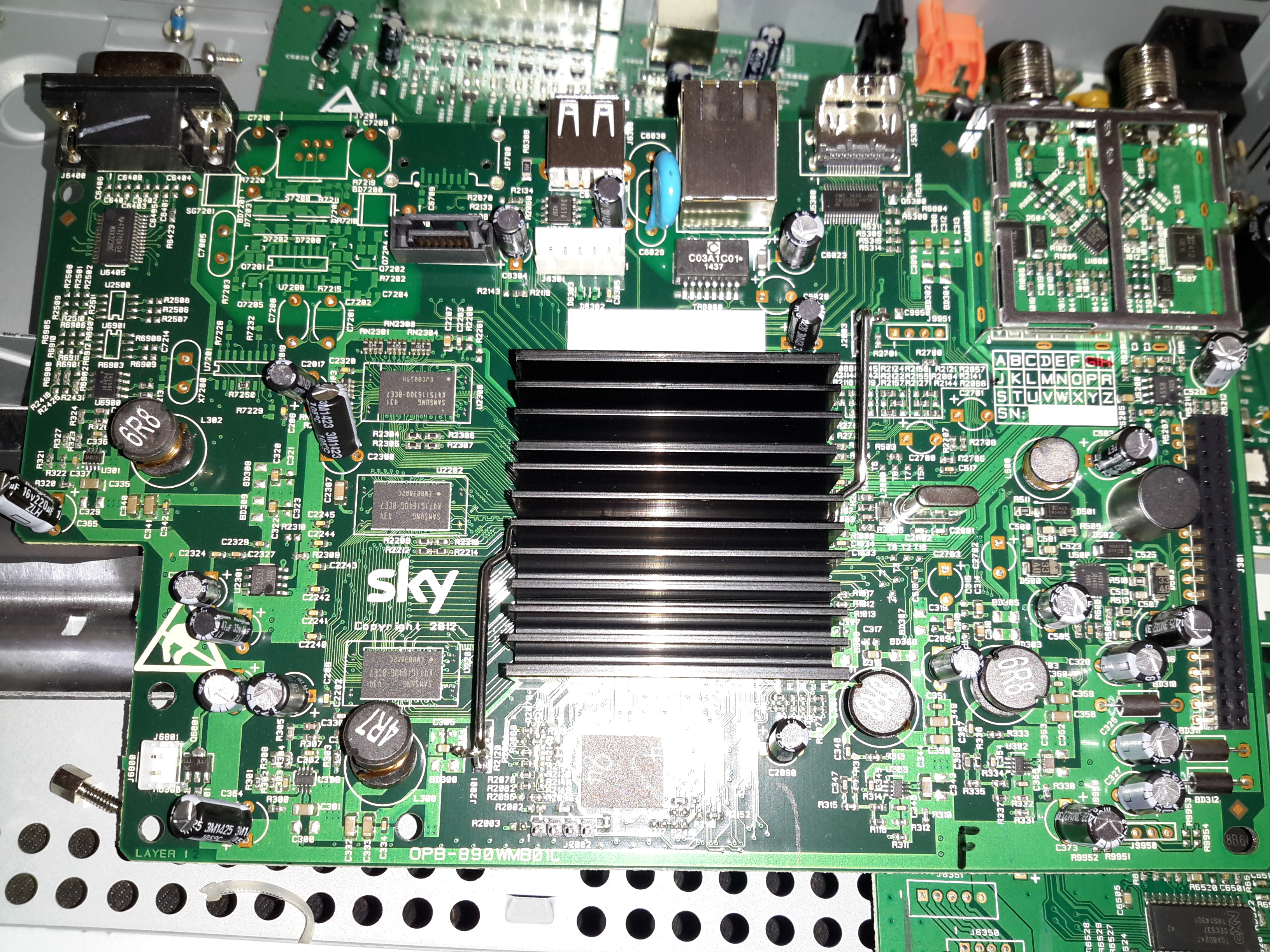
Here’s the main logic PCB. The massive heatsink in the middle is cooling the main SoC, below.
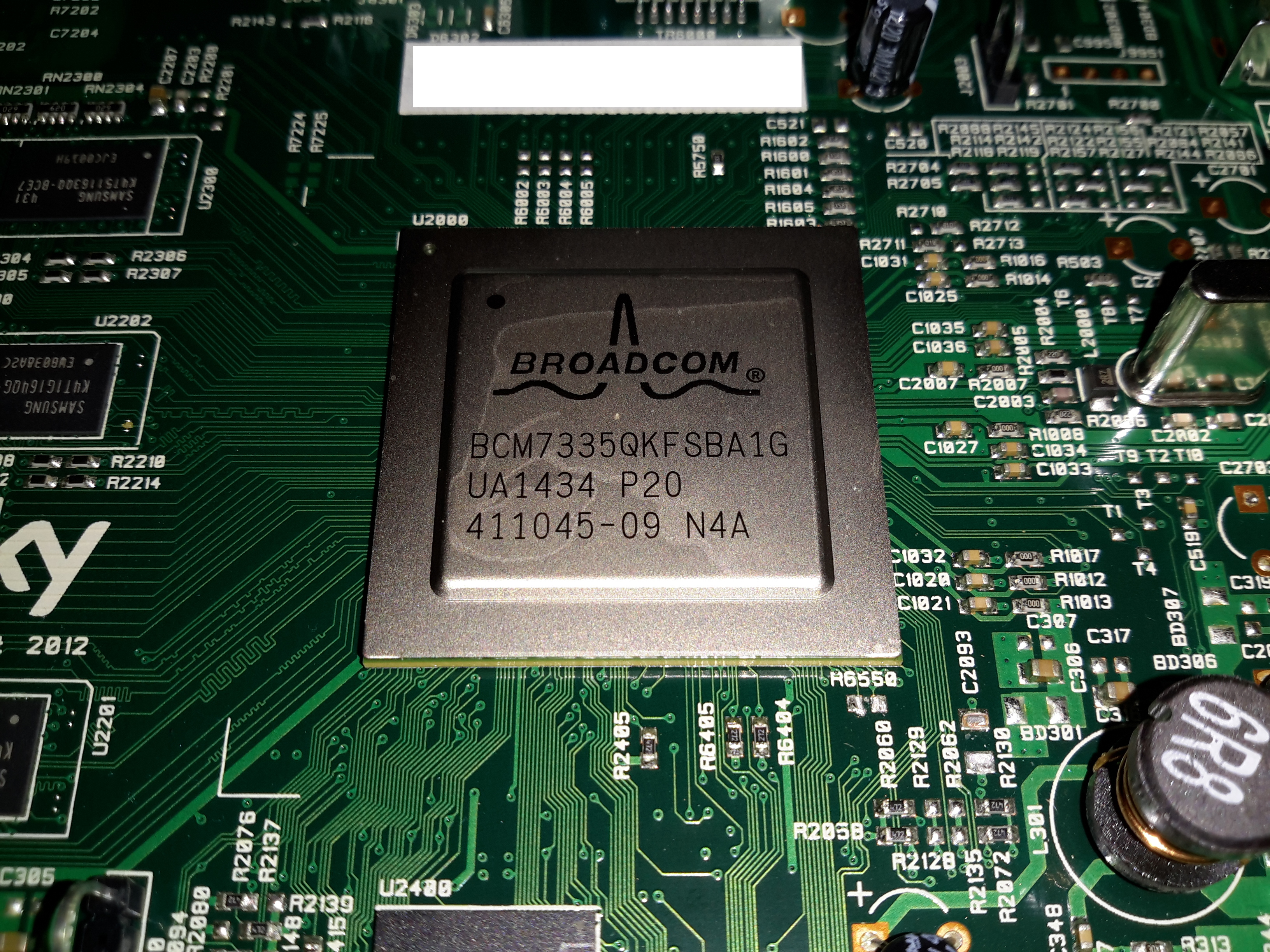
SoC
The main SoC in this unit is a Broadcom BCM7335 HD PVR Satellite System-On-Chip. It’s surrounded by it’s boot flash, a Spansion GL512P10FFCR1 512Mbit NOR device. It’s also got some DRAM around the left edge.
Smart Card Reader
The smart card reader is on the PSU PCB, the controller here is an NXP TDA8024
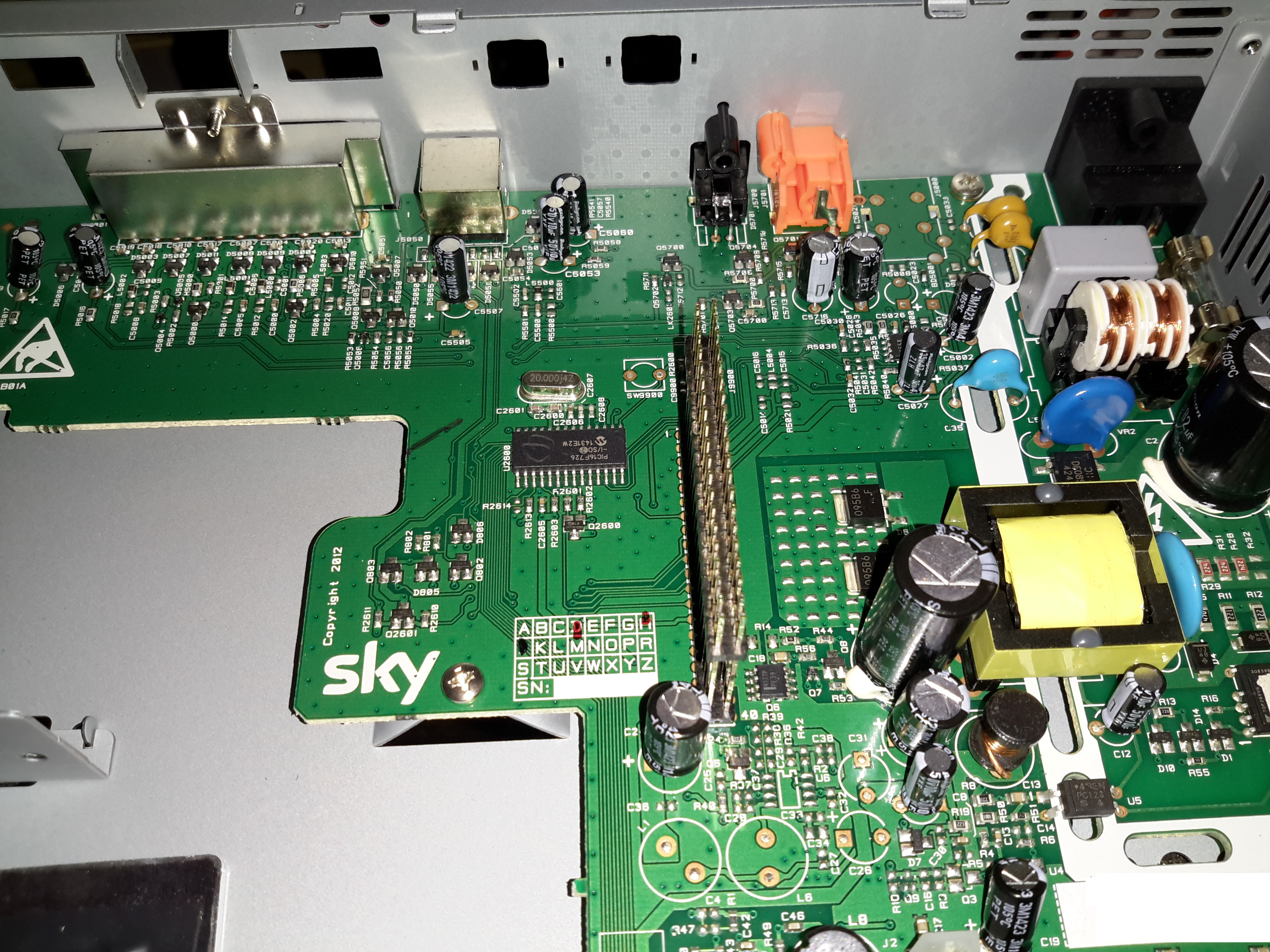
PSU PCB
The PSU itself is a pretty standard SMPS, so I won’t go too far into that particular bit. The logic PCB attaches to the large pin header on the left of the PSU, some of the analogue video outputs are also on this board.
There’s also a Microchip PIC16F726 microcontroller on this PCB, next to the pin header. Judging by the PCB traces, this handles everything on the user control panel.
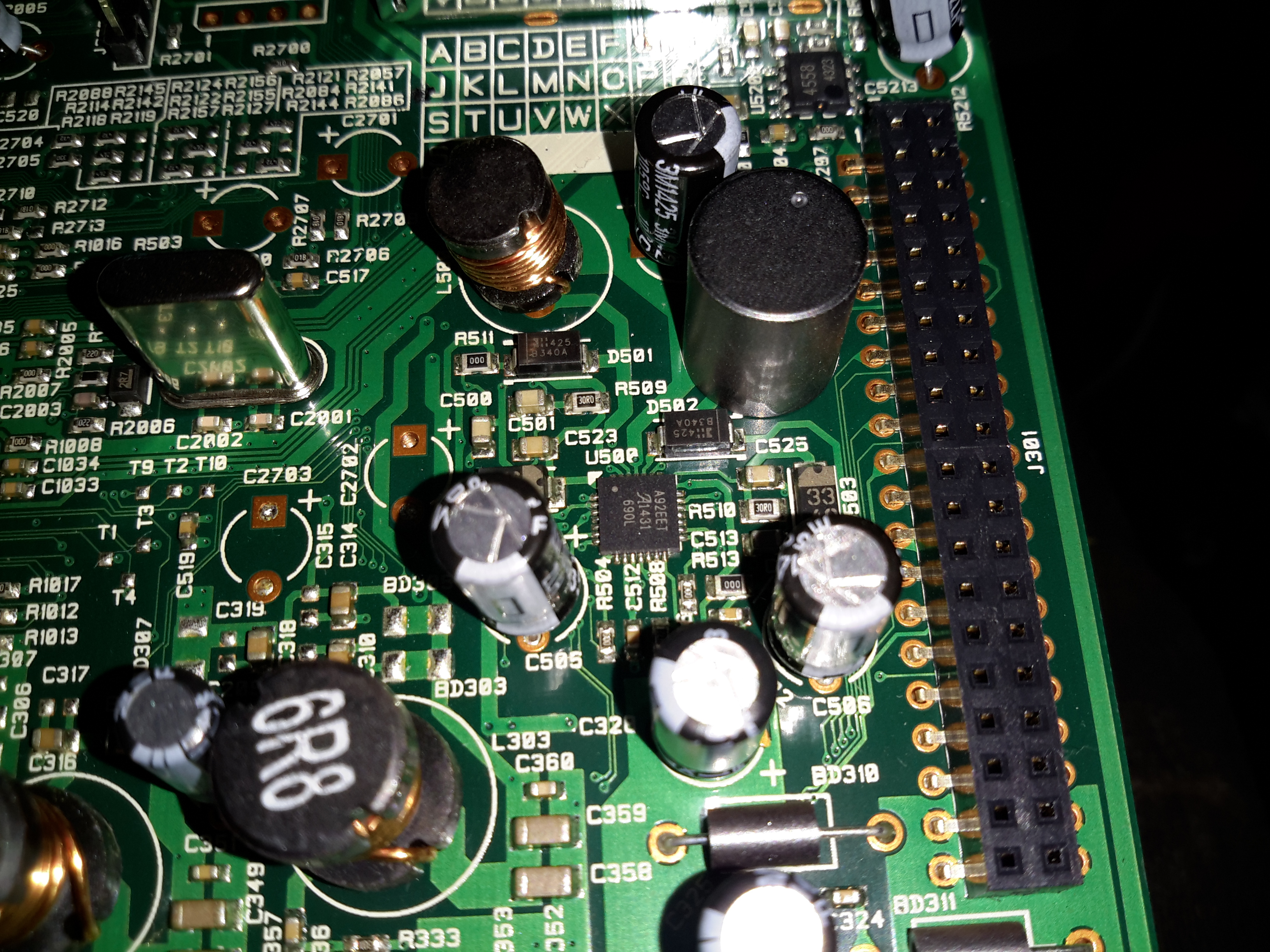
Power Supplies
Some local supplies are provided on the logic board for the main SoC, the IC in the centre here is an Allegro A92 DC-DC converter. I didn’t manage to find a datasheet for this one.
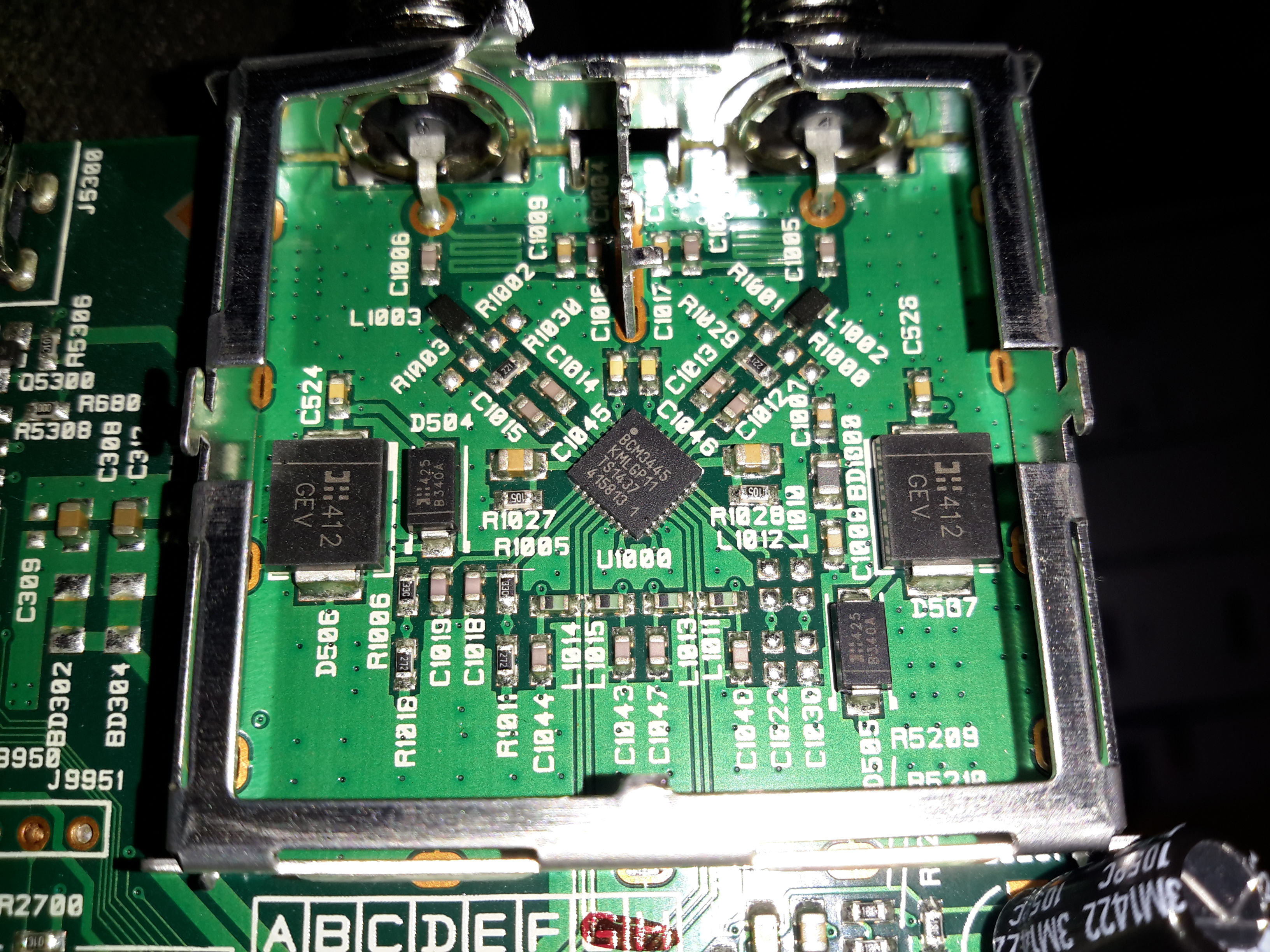
LNB Front End
The RF front end for the satellite input is a Broadcom BCM3445 Low Noise Amplifier & Splitter, again not much info on this one.
RS232 Section
The standard MAX232 is used for the serial interface. I imagine this is for diagnostics.
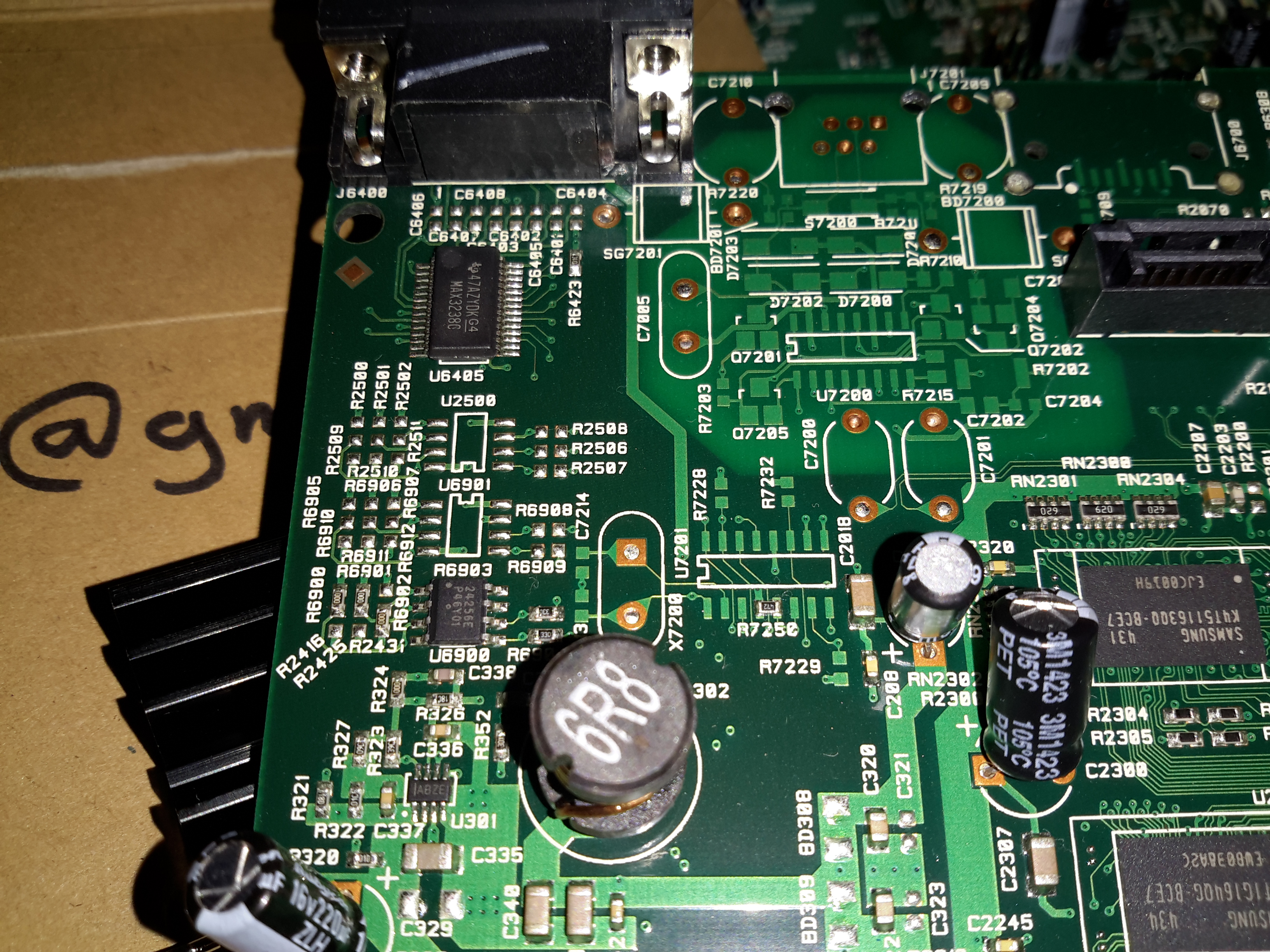
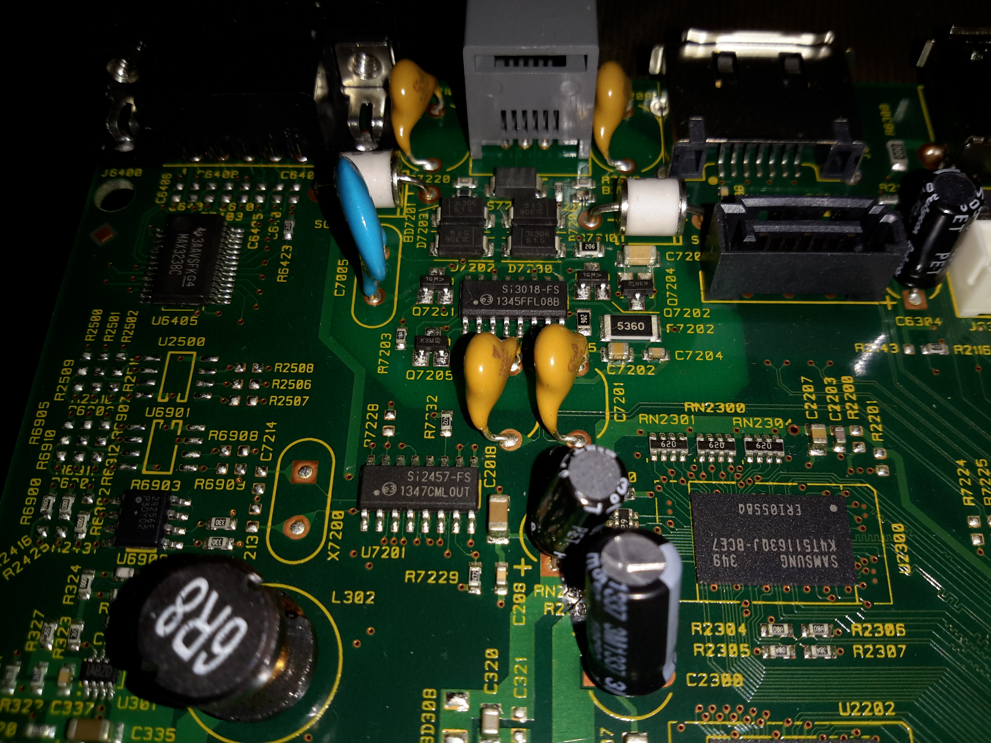
Modem
The POTS modem section is handled by a Si2457 System-Side device & Si3018 Line-Side device pair.
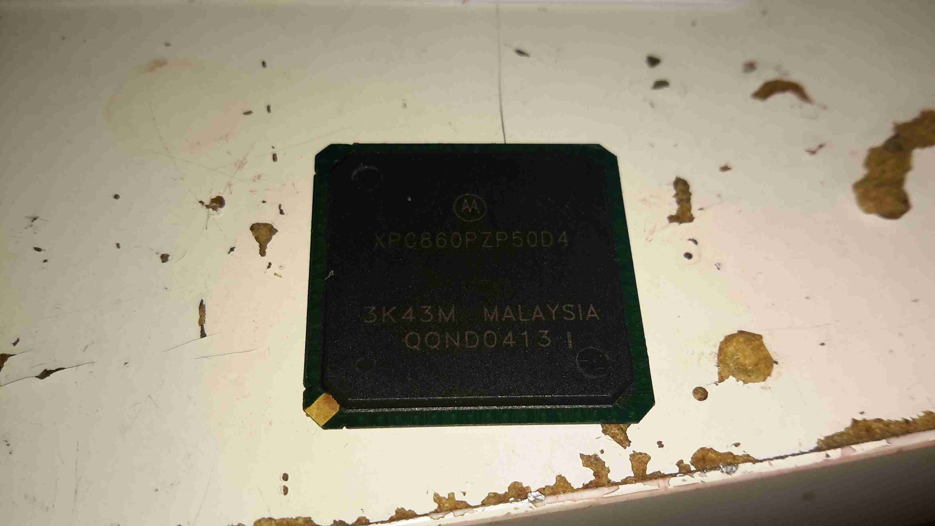
This is a System On Chip from Motorola, designed for network routing applications. This chip contains a hell of a feature set, so I’ll just include an excerpt from the datasheet:
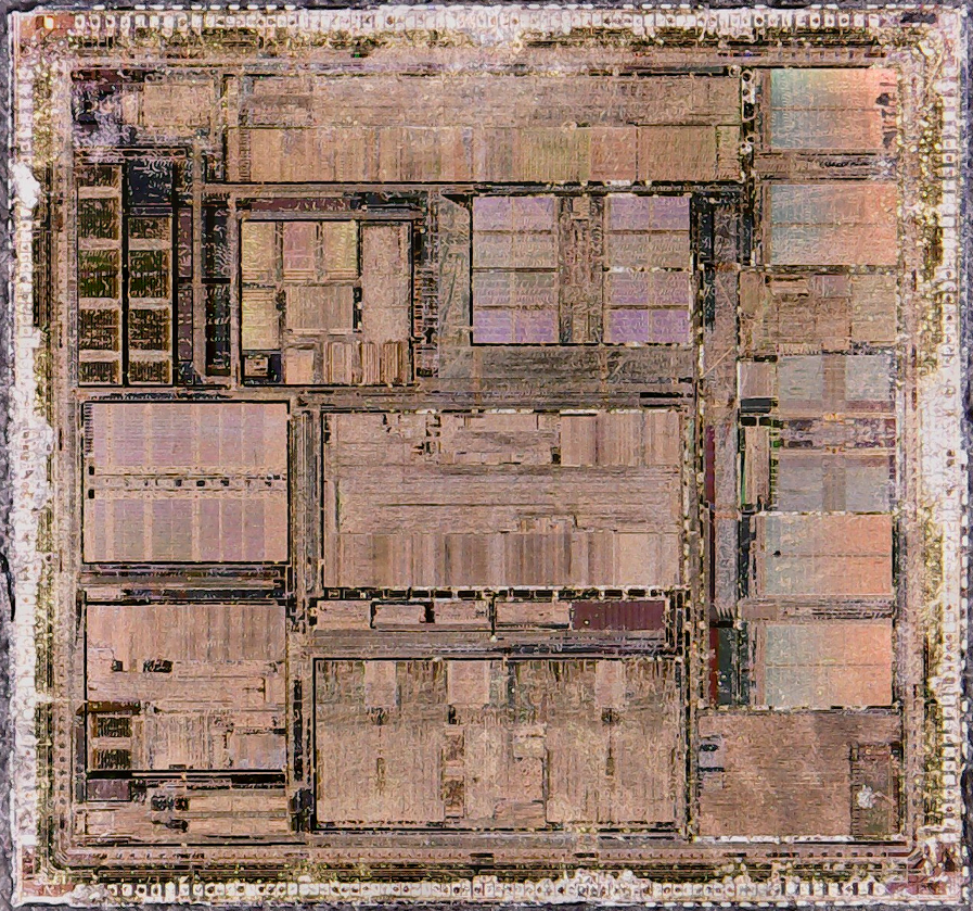
XPC860PZP50D4 Die
Embedded single-issue, 32-bit MPC8xx core (implementing the PowerPC
architecture) with thirty-two 32-bit general-purpose registers (GPRs)
— The core performs branch prediction with conditional prefetch, without
conditional execution
— 4- or 8-Kbyte data cache and 4- or 16-Kbyte instruction cache (see Table 1)
– 16-Kbyte instruction caches are four-way, set-associative with 256 sets;
4-Kbyte instruction caches are two-way, set-associative with 128 sets.
– 8-Kbyte data caches are two-way, set-associative with 256 sets; 4-Kbyte data
caches are two-way, set-associative with 128 sets.
– Cache coherency for both instruction and data caches is maintained on 128-bit
(4-word) cache blocks.
– Caches are physically addressed, implement a least recently used (LRU)
replacement algorithm, and are lockable on a cache block basis.
— Instruction and data caches are two-way, set-associative, physically addressed,
LRU replacement, and lockable on-line granularity.
— MMUs with 32-entry TLB, fully associative instruction, and data TLBs
— MMUs support multiple page sizes of 4, 16, and 512 Kbytes, and 8 Mbytes; 16
virtual address spaces and 16 protection groups
— Advanced on-chip-emulation debug mode
Up to 32-bit data bus (dynamic bus sizing for 8, 16, and 32 bits)
32 address lines
Operates at up to 80 MHz
Memory controller (eight banks)
— Contains complete dynamic RAM (DRAM) controller
— Each bank can be a chip select or RAS to support a DRAM bank
— Up to 15 wait states programmable per memory bank
— Glueless interface to DRAM, SIMMS, SRAM, EPROM, Flash EPROM, and
other memory devices.
— DRAM controller programmable to support most size and speed memory
interfaces
— Four CAS lines, four WE lines, one OE line
— Boot chip-select available at reset (options for 8-, 16-, or 32-bit memory)
— Variable block sizes (32 Kbyte to 256 Mbyte)
— Selectable write protection
— On-chip bus arbitration logic
General-purpose timers
— Four 16-bit timers or two 32-bit timers
— Gate mode can enable/disable counting
— Interrupt can be masked on reference match and event capture
System integration unit (SIU)
— Bus monitor
— Software watchdog
— Periodic interrupt timer (PIT)
— Low-power stop mode
— Clock synthesizer
— Decrementer, time base, and real-time clock (RTC) from the PowerPC
architecture
— Reset controller
— IEEE 1149.1 test access port (JTAG)
Interrupts
— Seven external interrupt request (IRQ) lines
— 12 port pins with interrupt capability
— 23 internal interrupt sources
— Programmable priority between SCCs
— Programmable highest priority request
10/100 Mbps Ethernet support, fully compliant with the IEEE 802.3u Standard (not
available when using ATM over UTOPIA interface)
ATM support compliant with ATM forum UNI 4.0 specification
— Cell processing up to 50–70 Mbps at 50-MHz system clock
— Cell multiplexing/demultiplexing
— Support of AAL5 and AAL0 protocols on a per-VC basis. AAL0 support enables
OAM and software implementation of other protocols).
— ATM pace control (APC) scheduler, providing direct support for constant bit rate
(CBR) and unspecified bit rate (UBR) and providing control mechanisms
enabling software support of available bit rate (ABR)
— Physical interface support for UTOPIA (10/100-Mbps is not supported with this
interface) and byte-aligned serial (for example, T1/E1/ADSL)
— UTOPIA-mode ATM supports level-1 master with cell-level handshake,
multi-PHY (up to 4 physical layer devices), connection to 25-, 51-, or 155-Mbps
framers, and UTOPIA/system clock ratios of 1/2 or 1/3.
— Serial-mode ATM connection supports transmission convergence (TC) function
for T1/E1/ADSL lines; cell delineation; cell payload scrambling/descrambling;
automatic idle/unassigned cell insertion/stripping; header error control (HEC)
generation, checking, and statistics.
Communications processor module (CPM)
— RISC communications processor (CP)
— Communication-specific commands (for example, GRACEFUL STOP TRANSMIT ,
ENTER HUNT MODE , and RESTART TRANSMIT )
— Supports continuous mode transmission and reception on all serial channels
— Up to 8Kbytes of dual-port RAM
— 16 serial DMA (SDMA) channels
— Three parallel I/O registers with open-drain capability
Four baud-rate generators (BRGs)
— Independent (can be connected to any SCC or SMC)
— Allow changes during operation
— Autobaud support option
Four serial communications controllers (SCCs)
— Ethernet/IEEE 802.3 optional on SCC1–4, supporting full 10-Mbps operation
(available only on specially programmed devices).
— HDLC/SDLC (all channels supported at 2 Mbps)
— HDLC bus (implements an HDLC-based local area network (LAN))
— Asynchronous HDLC to support PPP (point-to-point protocol)
— AppleTalk
— Universal asynchronous receiver transmitter (UART)
— Synchronous UART
— Serial infrared (IrDA)
— Binary synchronous communication (BISYNC)
— Totally transparent (bit streams)
— Totally transparent (frame based with optional cyclic redundancy check (CRC))
Two SMCs (serial management channels)
— UART
— Transparent
— General circuit interface (GCI) controller
— Can be connected to the time-division multiplexed (TDM) channels
One SPI (serial peripheral interface)
— Supports master and slave modes
— Supports multimaster operation on the same bus
One I 2 C (inter-integrated circuit) port
— Supports master and slave modes
— Multiple-master environment support
Time-slot assigner (TSA)
— Allows SCCs and SMCs to run in multiplexed and/or non-multiplexed operation
— Supports T1, CEPT, PCM highway, ISDN basic rate, ISDN primary rate, user
defined
— 1- or 8-bit resolution
— Allows independent transmit and receive routing, frame synchronization,
clocking
— Allows dynamic changes
— Can be internally connected to six serial channels (four SCCs and two SMCs)
Parallel interface port (PIP)
— Centronics interface support
— Supports fast connection between compatible ports on the MPC860 or the
MC68360
PCMCIA interface
— Master (socket) interface, release 2.1 compliant
— Supports two independent PCMCIA sockets
— Eight memory or I/O windows supported
Low power support
— Full on—all units fully powered
— Doze—core functional units disabled, except time base decrementer, PLL,
memory controller, RTC, and CPM in low-power standby
— Sleep—all units disabled, except RTC and PIT, PLL active for fast wake up
— Deep sleep—all units disabled including PLL, except RTC and PIT
— Power down mode— all units powered down, except PLL, RTC, PIT, time base,
and decrementer
Debug interface
— Eight comparators: four operate on instruction address, two operate on data
address, and two operate on data
— Supports conditions: = ≠ < >
— Each watchpoint can generate a break-point internally
3.3 V operation with 5-V TTL compatibility except EXTAL and EXTCLK
357-pin ball grid array (BGA) package
Tip Jar
If you’ve found my content useful, please consider leaving a donation by clicking the Tip Jar below!
All collected funds go towards new content & the costs of keeping the server online.