After watching a video over at Scullcom Hobby Electronics on YouTube, I figured I’d build one of these precision references to calibrate my multimeters.
It’s based around a REF102P 10v precision reference & an INA105P precision unity gain differential amplifier.
For full information, check out the video, I won’t go into the details here, just my particular circuit & PCB layout.
In the video, Veroboard is used. I’m not too fond of the stuff personally. I find it far too easy to make mistakes & it never quite looks good enough. To this end I have spun a board in Eagle, as usual.
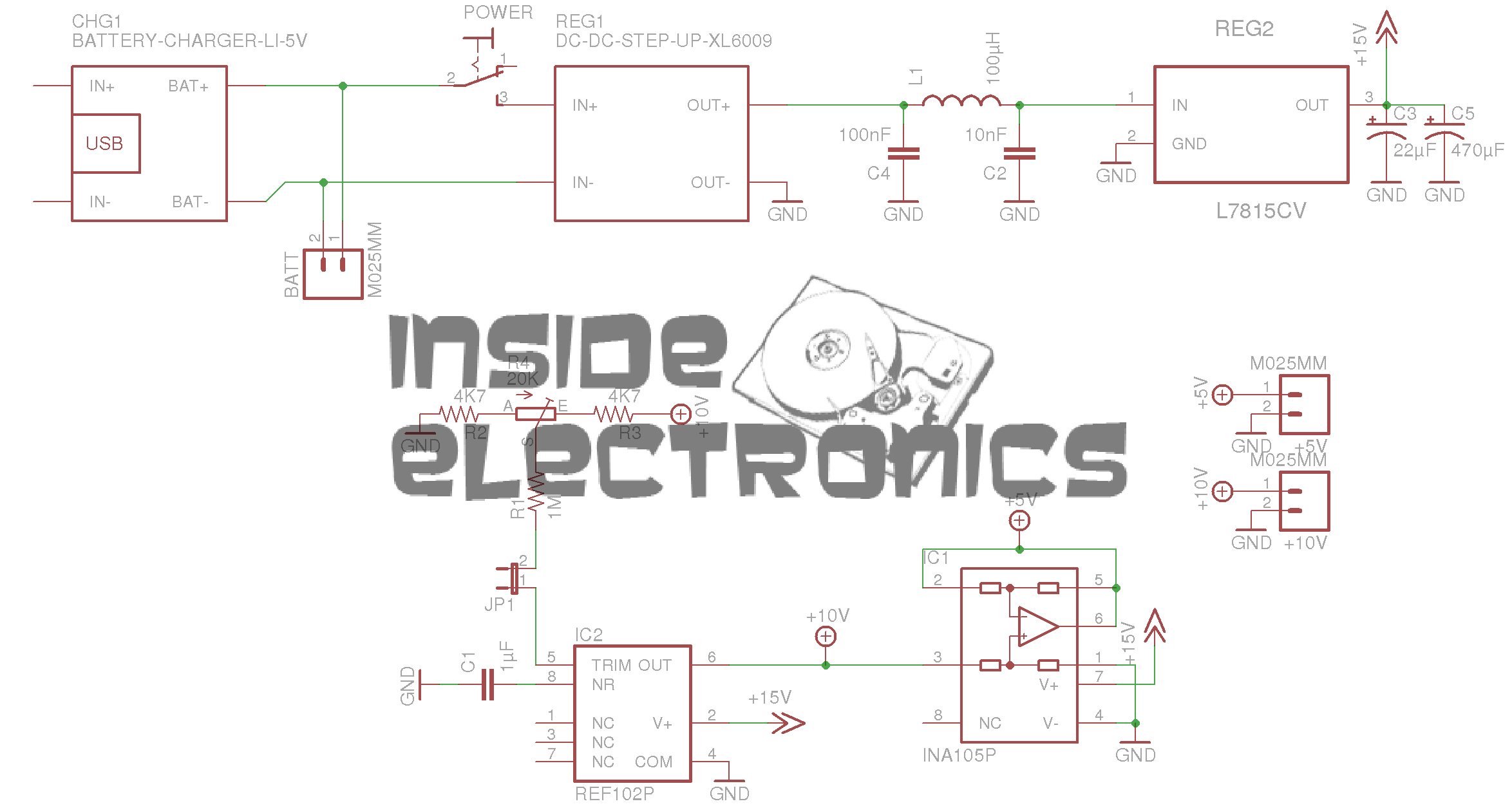
Here’s the schematic layout, the same as is in the video.
As usual, the Eagle CAD layout files can be found at the bottom of the post.
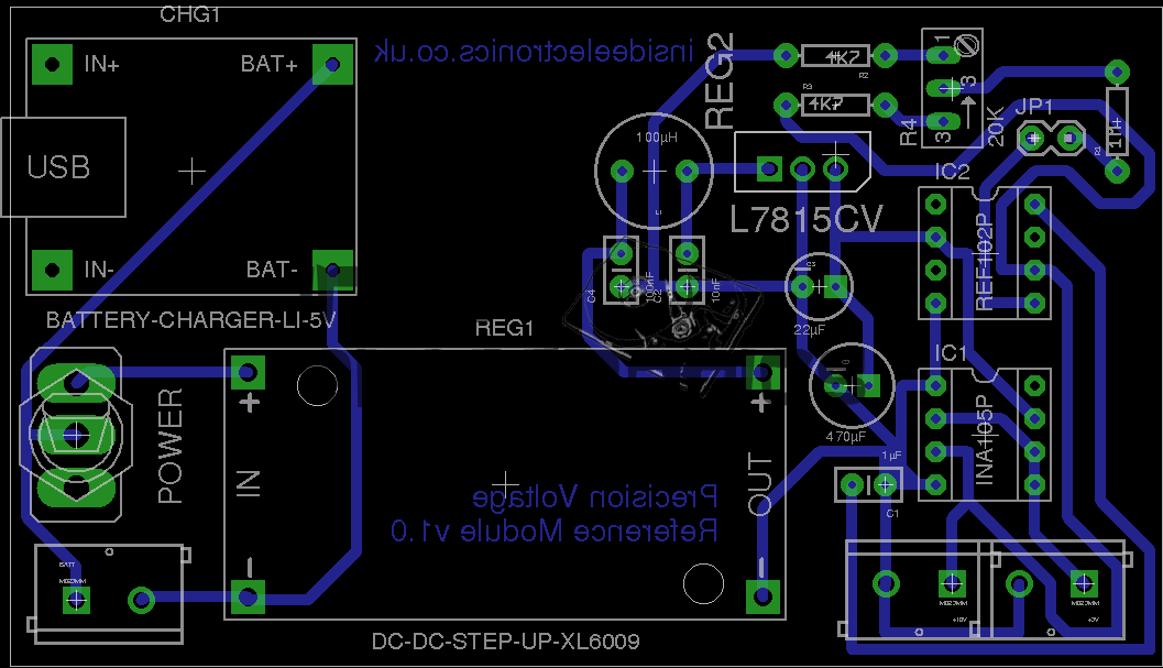
And the associated PCB layout. I have added the option to be able to tweak the output, to get a more accurate calibration, which can be added by connecting JP1 on the PCB.
As in the original build, this unit uses pre-built DC-DC converter & Li-Ion charger modules. A handy Eagle library can be found online for these parts.
I have however left off the battery monitor section of the circuit, since I plan to use a protected lithium cell for power. This also allowed me to keep the board size down, & use a single sided layout.
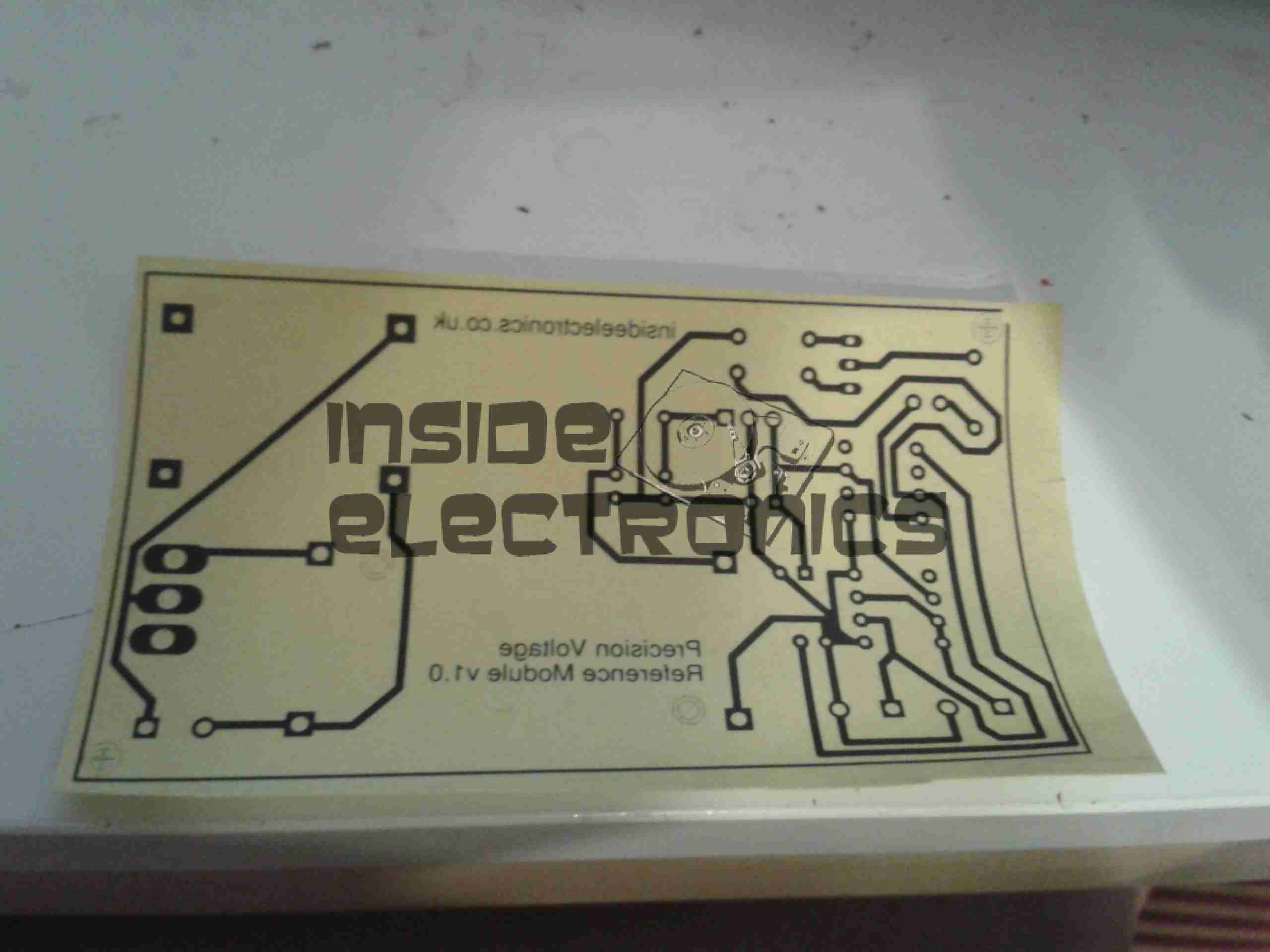
Here’s the track layout ready to iron onto the copper clad board. I use the popular toner transfer system with special paper from eBay, this stuff has a coating that allows the toner to easily be transferred to the PCB without having to mess about with soaking in water & scraping paper off.
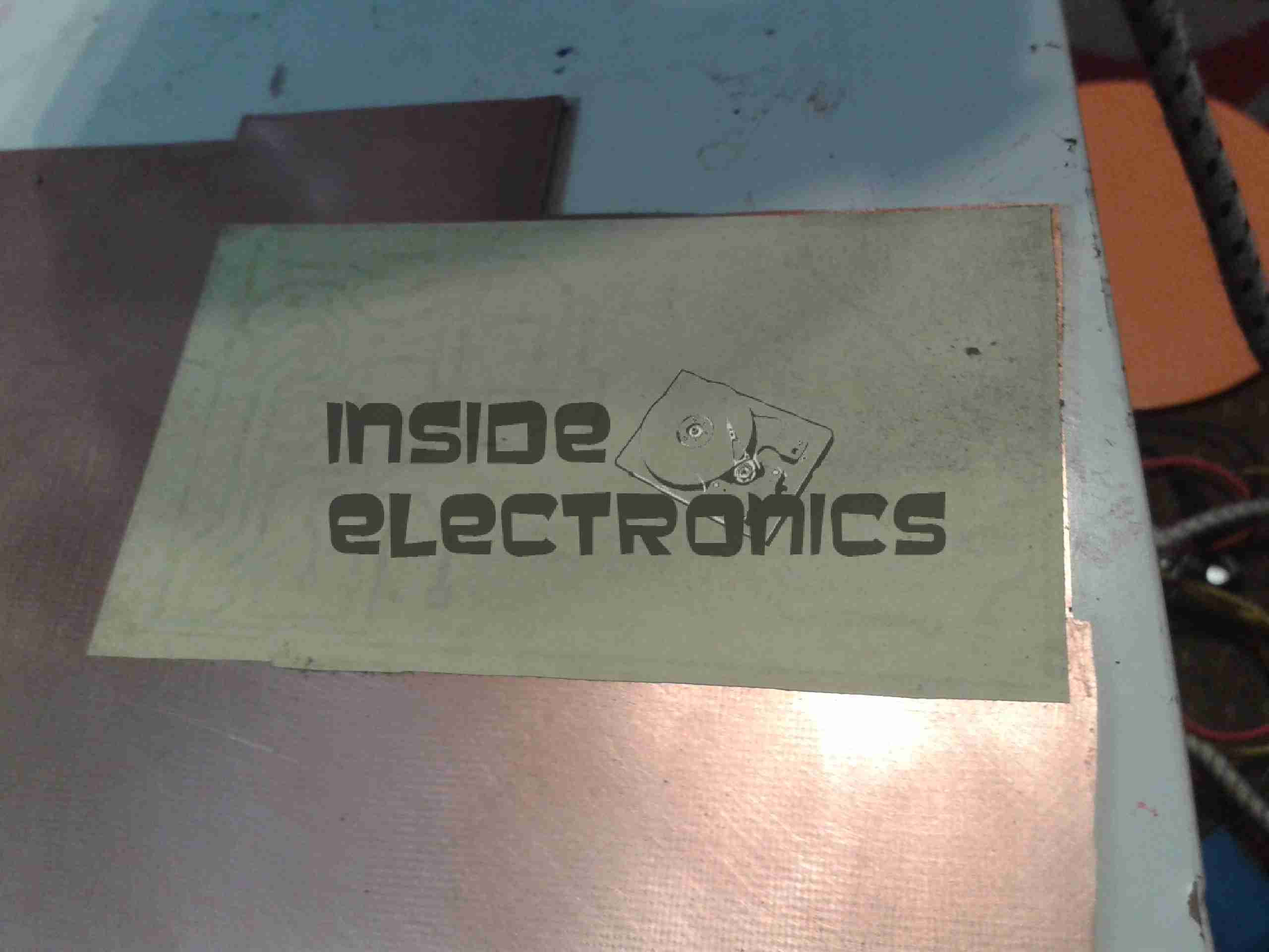
Here’s the paper having just been ironed onto the copper. After waiting for the board to cool off the paper is peeled off, leaving just the toner on the PCB.
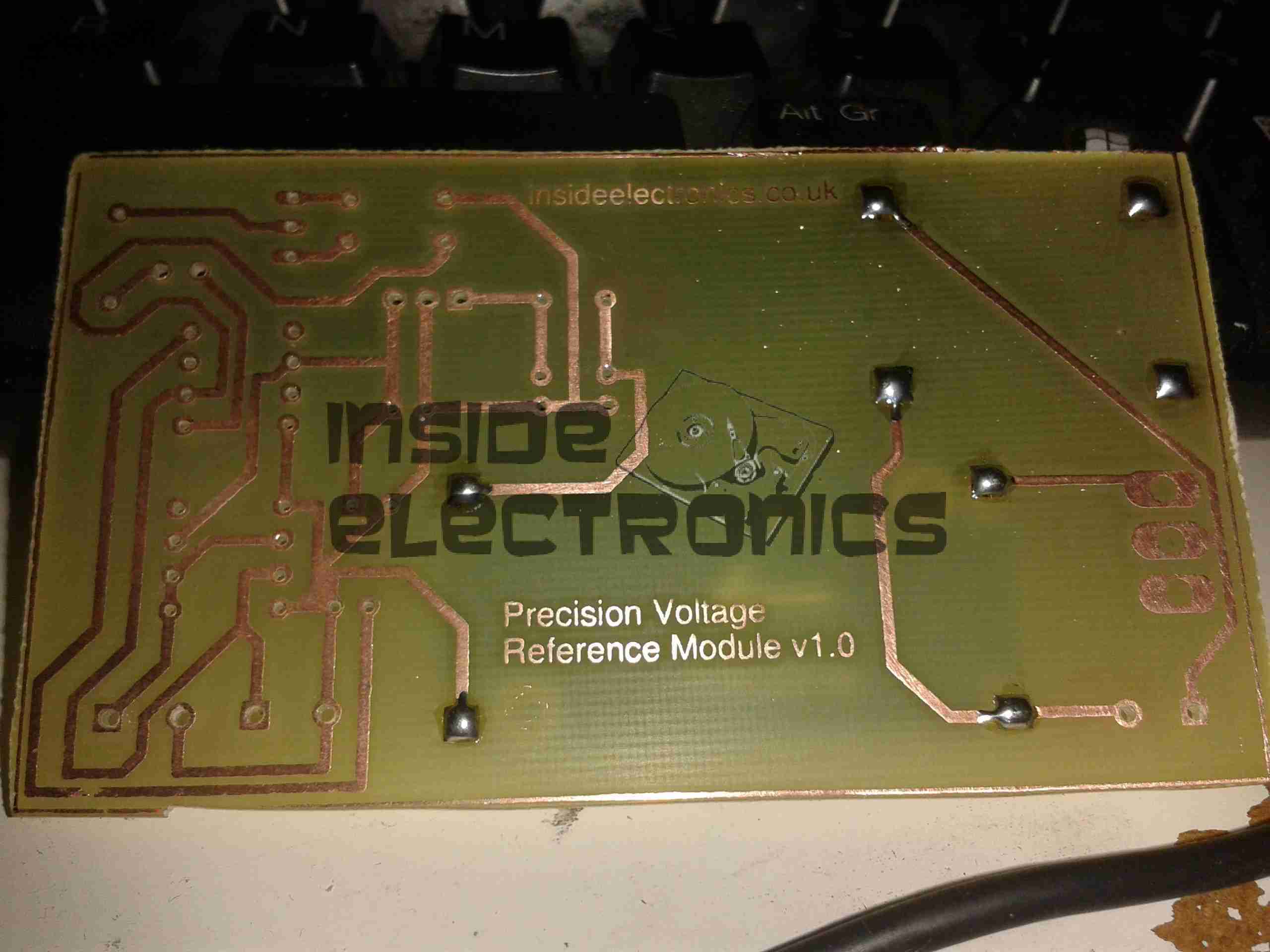
PCB just out of the etch tank, drilled & with the solder pins for the modules installed. Only one issue with the transfer, in the bottom left corner of the board is visible, a very small section of copper was over etched.
This is easily fixed with a small piece of wire.
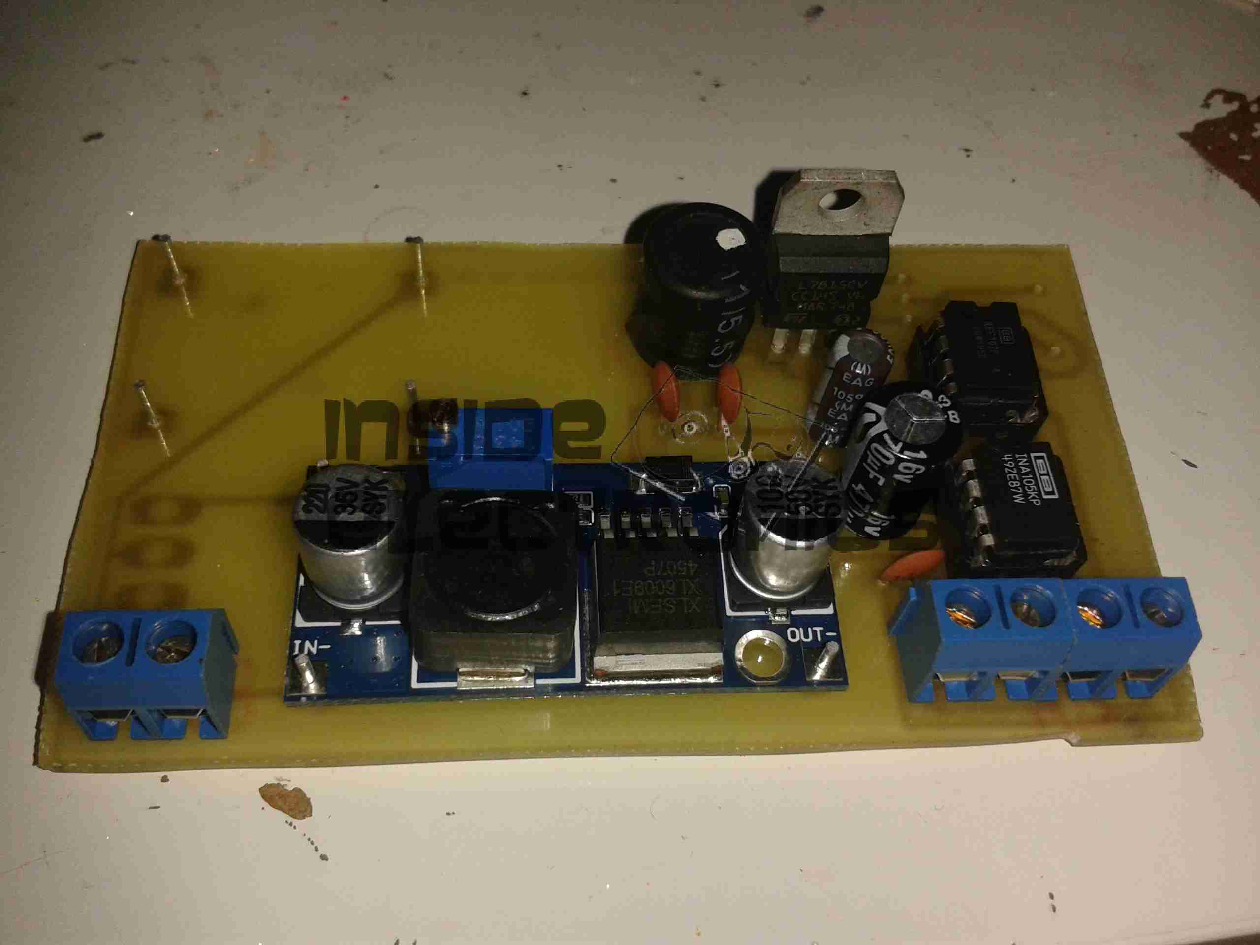
Main components populated. The DC-DC converter is set at 24v output, which the linear regulator then drops down to the +15v rail for the reference IC. The linear section of the regulator, along with the LC filter on the output of the switching regulator produce a low-ripple supply.
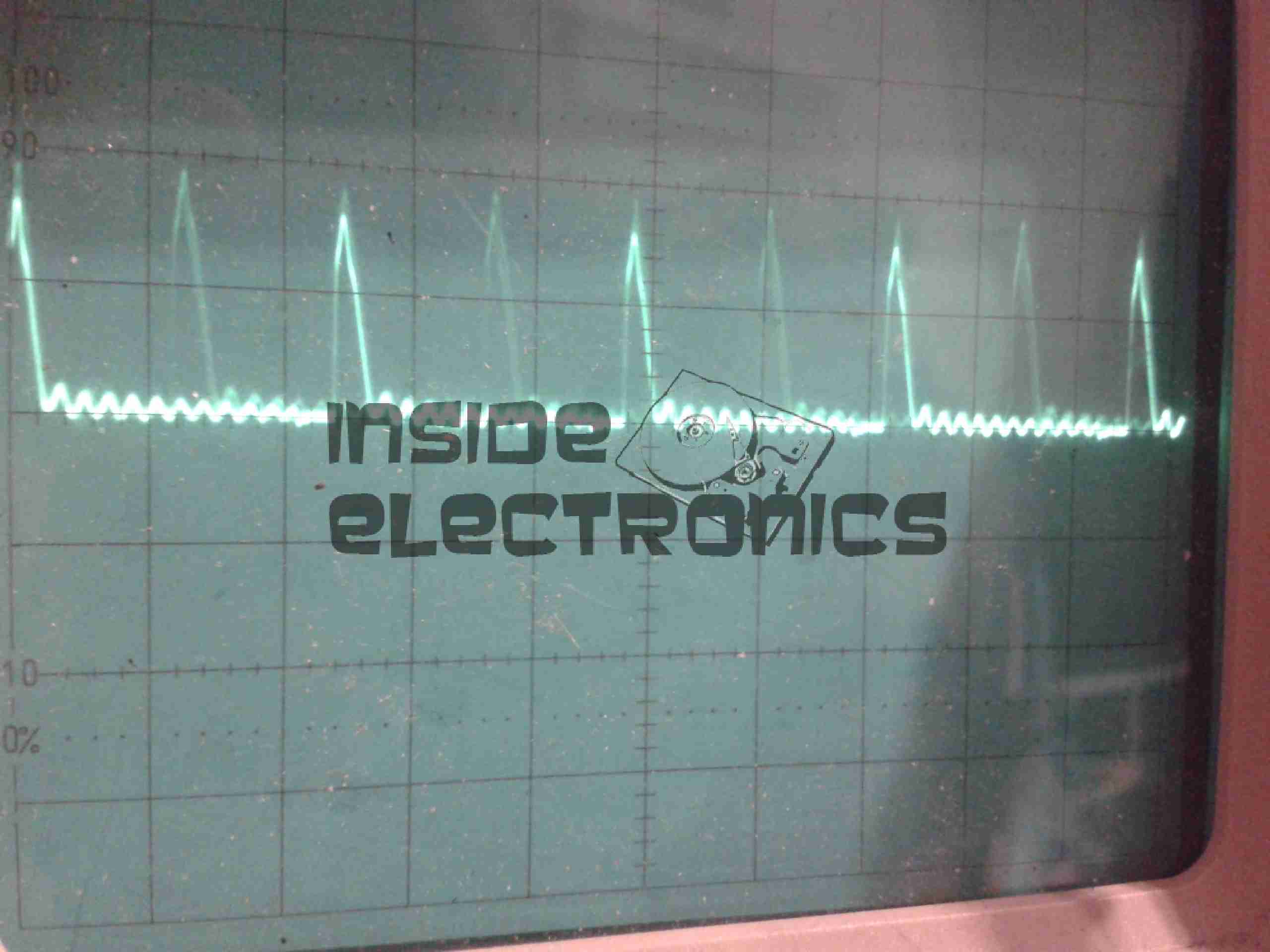
Here’s the scope reading the AC ripple on the output of the DC-DC converter. Scale is 100mV/Div. Roughly 150mV of ripple is riding on top of the DC rail.
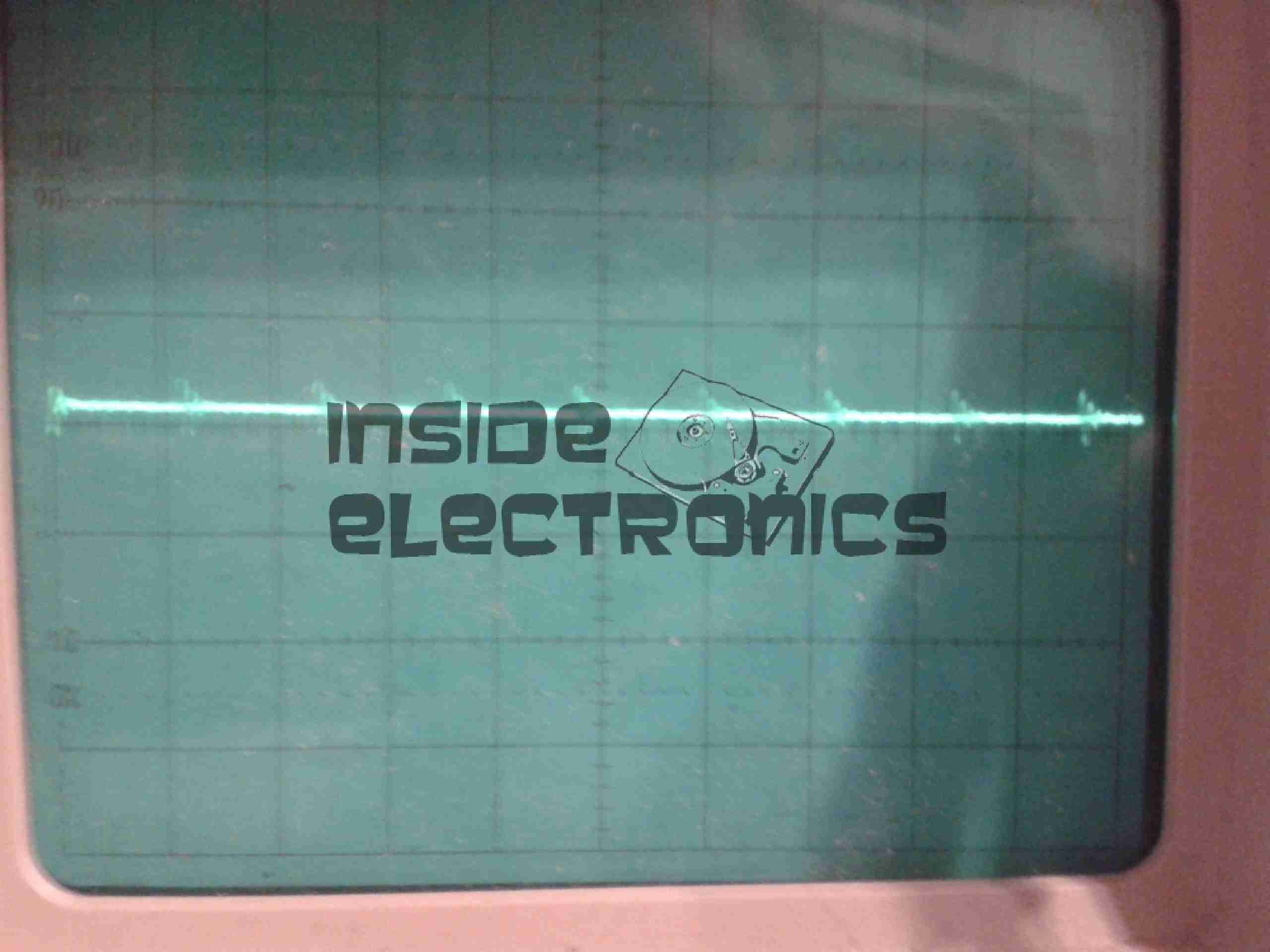
And here’s the output from the linear regulator, scale of 50mV/Div. Ripple has been reduced to ~15mV for the reference IC.
In total the circuit as built has a power consumption of ~0.5W, most of which is being dissipated as heat in the linear part of the PSU.
[download id=”5583″]
