Posted on 2 Comments

PowerAdd Pilot X7 20,000mAh Powerbank & Fast Charging Mod

PowerAdd Pilot X7
PowerAdd Pilot X7

Here’s the biggest portable USB powerbank I’ve seen yet – the PowerAdd Pilot X7, this comes with a 20Ah (20,000mAh) capacity. This pack is pretty heavy, but this isn’t surprising considering the capacity.
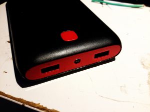
USB Ports & LED
USB Ports & LED

The front of the pack houses the usual USB ports, in this case rated at 3.4A total between the ports. There’s a white LED in the centre as a small torch, activated by double-clicking the button. A single click of the button lights up the 4 blue LEDs under the housing that indicate remaining battery capacity. Factory charging is via a standard µUSB connector in the side, at a maximum of 2A.
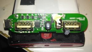
PCB Front
PCB Front

The front of the PCB holds the USB ports, along with most of the main control circuitry. At top left is a string of FS8025A dual-MOSFETs all in parallel for a current carrying capacity of 15A total, to the right of these is the ubiquitous DW01 Lithium-Ion protection IC. These 4 components make up the battery protection – stopping both an overcharge & overdischarge. The larger IC below is an EG1501 multi-purpose power controller.

This chip is doing all of the heavy lifting in this power pack, dealing with all the DC-DC conversion for the USB ports, charge control of the battery pack, controlling the battery level indicator LEDs & controlling the torch LED in the centre.
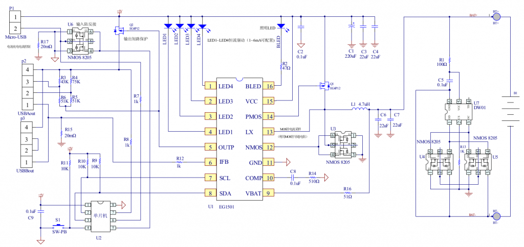
EG1501 Example
EG1501 Example

The datasheet is in Chinese, but it does have an example application circuit, which is very similar to the circuitry used in this powerbank. A toroidal inductor is nestled next to the right-hand USB port for the DC-DC converter, and the remaining IC next to it is a CW3004 Dual-Channel USB Charging Controller, which automatically sets the data pins on the USB ports to the correct levels to ensure high-current charging of the devices plugged in. This IC replaces the resistors R3-R6 in the schematic above.
The DC-DC converter section of the power chain is designed with high efficiency in mind, not using any diodes, but synchronous rectification instead.
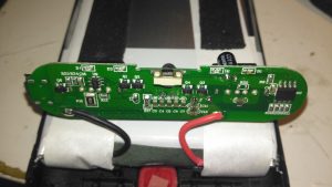
PCB Back
PCB Back

The back of the PCB just has a few discrete transistors, the user interface button, and a small SO8 IC with no markings at all. I’m going to assume this is a generic microcontroller, (U2 in the schematic) & is just there to interface the user button to the power controller via I²C.
Cells
Cells

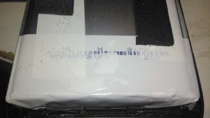
Not many markings on the cells indicating their capacity, but a full discharge test at 4A gave me a resulting capacity of 21Ah – slightly above the nameplate rating. There are two cells in here in parallel, ~10Ah capacity each.
XT60 Battery Connector

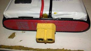
The only issue with powerbanks this large is the amount of time they require to recharge themselves – at this unit’s maximum of 2A through the µUSB port, it’s about 22 hours! Here I’ve fitted an XT60 connector, to interface to my Turnigy Accucell 6 charger, increasing the charging current capacity to 6A, and reducing the full-charge time to 7 hours. This splits to 3A charge per cell, and after some testing the cells don’t seem to mind this higher charging current.
Battery Connector Wiring

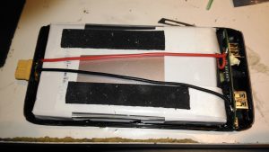
The new charging connector is directly connected to the battery at the control PCB, there’s just enough room to get a pair of wires down the casing over the cells.
Posted on 1 Comment

Panasonic NV-M5 CRT Viewfinder Hack

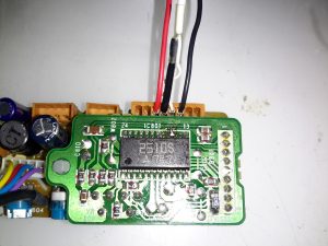
Viewfinder Circuits
Viewfinder Circuits


The old Panasonic NV-M5 has the standard for the time CRT based viewfinder assembly, which will happily take a composite video signal from an external source.

This viewfinder has many more connections than I would have expected, as it has an input for the iris signal, which places a movable marker on the edge of the display. This unit also has a pair of outputs for the vertical & horizontal deflection signals, I imagine for sync, but I’ve never seen these signals as an output on a viewfinder before.

EVF Schematic
EVF Schematic

Luckily I managed to get a service manual for the camera with a full schematic.
This unit takes a 5v input, as opposed to the 8-12v inputs on previous cameras, so watch out for this! There’s also no reverse polarity protection either.

Pins
Pins

Making the iris marker vanish from the screen is easy, just put a solder bridge between pins 15 & 16 of the drive IC. The important pins on the interface connector are as follows:

Pin 3: GND
Pin 4: Video Input
Pin 5: Video GND
Pins 6: +5v Supply

Posted on Leave a comment

Mini USB Soldering Iron

USB Soldering Iron
USB Soldering Iron

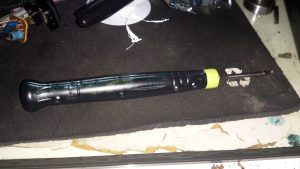
Here’s a novel little gadget, a USB powered soldering iron. The heating tip on these is very small & might be useful for very small SMD work. Bigger joints not so much, as it’s only rated at 8W. (Still breaks the USB standard of 2.5W from a single port).

These irons aren’t actually too bad to use, as long as the limitations in power are respected. Since nearly everything has a USB power port these days, it could make for a handy emergency soldering iron.

Heater Socket
Heater Socket

The heater & soldering bit are a single unit, not designed to be replaced separately. (I’ve not managed to find replacement elements, but at £3 for the entire iron, it would be pretty pointless).
Above is the socket where the heater plugs in, safely isolating the plastic body from any stray heat.

DC Input Jack
DC Input Jack

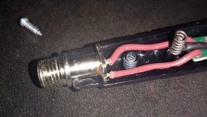
The DC input is a 3.5mm audio jack, a non-standard USB to 3.5mm jack cable is supplied. Such non-standard cables have the potential to damage equipment that isn’t expecting to see 5v on an audio input if it’s used incorrectly.

Touch Sensor & LED
Touch Sensor & LED

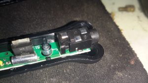
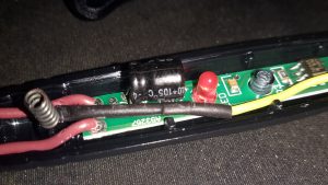
There isn’t actually a switch on this unit for power management, but a clever arrangement of a touch button & vibration switch. The vertical spring in the photo above makes contact with a steel ball bearing pressed into the plastic housing, forming the touch contact.

MOSFET
MOSFET

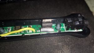
The large MOSFET here is switching the main heater current, the silver cylinder in front is the vibration switch, connected in parallel with the touch button.

PCB
PCB

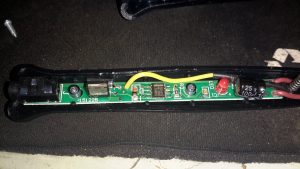
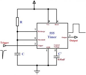
The main controller is very simple. It’s a 555 timer configured in monostable mode. Below is a schematic showing the basic circuit.

555 Monostable
555 Monostable

Big Clive also did a teardown & review of this iron. Head over to YouTube to watch.

Posted on Leave a comment

Maplin/Refrakta Torch Modification & Mode Removal

The multimode dimming/flashing modes on Chinese torches have irritated me for a while. If I buy a torch, it’s to illuminate something I’m doing, not to test if people around me have photosensitive epilepsy.

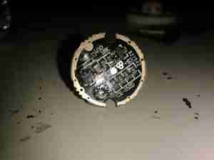
Looking at the PCB in the LED module of the torch, a couple of components are evident:

LED Driver PCB
LED Driver PCB

There’s not much to this driver, it’s simply resistive for LED protection (the 4 resistors in a row at the bottom of the board).
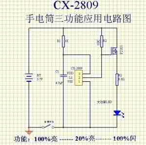
The components at the top are the multimode circuitry. The SOT-23 IC on the left is a CX2809 LED Driver, with several modes. The SOT-23 on the right is a MOSFET, for switching the actual LED itself. I couldn’t find a datasheet for the IC itself, but I did find a schematic that seems to match up with what’s on the board.

Schematic
Schematic

Here’s that schematic, the only thing that needs to be done to convert the torch to single mode ON/OFF at full brightness, is to bridge out that FET.

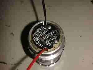
Components Desoldered

To help save the extra few mA the IC & associated circuitry will draw from the battery, I have removed all of the components involved in the multimode control. This leaves just the current limiting resistors for the LED itself.

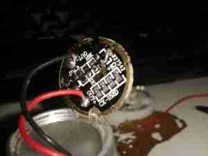
Jumper Link
Jumper Link

The final part above, is to install a small link across the Drain & Source pads of the FET. Now the switch controls the LED directly with no silly electronics in between. A proper torch at last.

Posted on Leave a comment

Rigol DS1054Z 12v Power Supply Noise Filtering

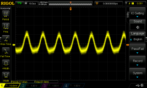
Since I fitted my scope with a SMPS based 12v input supply, there has been a noise problem on very low volts/div settings, this noise isn’t present on the mains supply, so I can only think it’s coming from the switching frequencies of the various DC-DC modules I’ve used.

Scope Ripple
Scope Ripple

Because of this I’ve designed a linear post-regulation stage for the supply, to remove the RFI from the DC rails.
This board takes the outputs from the DC-DC converters, removes all the noise & outputs clean DC onto the mainboard of the scope.

As the scope internally uses regulation to get the voltages lower, I’ve found that I don’t have to match the outputs of the mains supply exactly, for the +/-17.5v rails, 12v is perfectly fine instead.

Scope Linear PSU
Scope Linear PSU

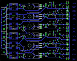
Here’s the PCB layout, with the 6  common mode filters on the input (left), linear regulator ICs in the centre & the output filters on the right.

Scope Linear PSU
Scope Linear PSU

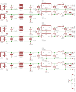
Here’s the schematic layout, as usual the Eagle Project files are in the link below, I’ll update when I have built the board & tested!

[download id=”5589″]

73s for now 🙂

Posted on Leave a comment

Precision 10v & 5v Reference

After watching a video over at Scullcom Hobby Electronics on YouTube, I figured I’d build one of these precision references to calibrate my multimeters.
It’s based around a REF102P 10v precision reference & an INA105P precision unity gain differential amplifier.
For full information, check out the video, I won’t go into the details here, just my particular circuit & PCB layout.

In the video, Veroboard is used. I’m not too fond of the stuff personally. I find it far too easy to make mistakes & it never quite looks good enough. To this end I have spun a board in Eagle, as usual.

Precision Ref SCH
Precision Ref SCH – Click to Embiggen

Here’s the schematic layout, the same as is in the video.

Precision Ref BRD
Precision Ref BRD

As usual, the Eagle CAD layout files can be found at the bottom of the post.

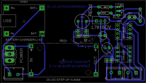
And the associated PCB layout. I have added the option to be able to tweak the output, to get a more accurate calibration, which can be added by connecting JP1 on the PCB.

As in the original build, this unit uses pre-built DC-DC converter & Li-Ion charger modules. A handy Eagle library can be found online for these parts.
I have however left off the battery monitor section of the circuit, since I plan to use a protected lithium cell for power. This also allowed me to keep the board size down, & use a single sided layout.

Toner Transfer Paper

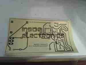
Here’s the track layout ready to iron onto the copper clad board. I use the popular toner transfer system with special paper from eBay, this stuff has a coating that allows the toner to easily be transferred to the PCB without having to mess about with soaking in water & scraping paper off.

Ironed On
Ironed On

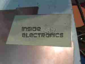
Here’s the paper having just been ironed onto the copper. After waiting for the board to cool off the paper is peeled off, leaving just the toner on the PCB.

Etched PCB
Etched PCB

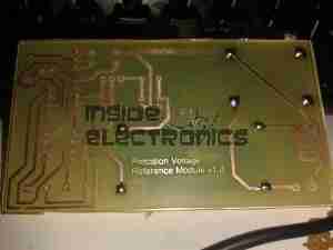
PCB just out of the etch tank, drilled & with the solder pins for the modules installed. Only one issue with the transfer, in the bottom left corner of the board is visible, a very small section of copper was over etched.
This is easily fixed with a small piece of wire.

Components Populated

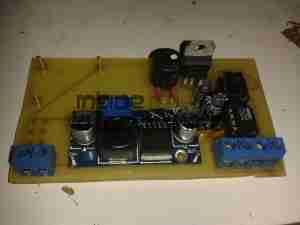
Main components populated. The DC-DC converter is set at 24v output, which the linear regulator then drops down to the +15v rail for the reference IC. The linear section of the regulator, along with the LC filter on the output of the switching regulator produce a low-ripple supply.

SMPS Ripple
SMPS Ripple

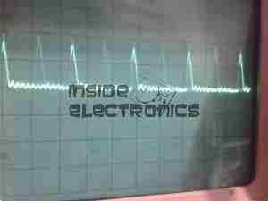
Here’s the scope reading the AC ripple on the output of the DC-DC converter. Scale is 100mV/Div. Roughly 150mV of ripple is riding on top of the DC rail.

Linear PSU Ripple
Linear PSU Ripple

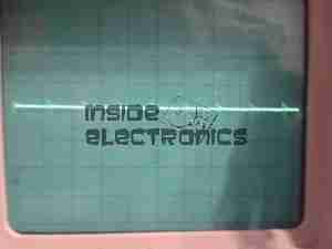
And here’s the output from the linear regulator, scale of 50mV/Div. Ripple has been reduced to ~15mV for the reference IC.
In total the circuit as built has a power consumption of ~0.5W, most of which is being dissipated as heat in the linear part of the PSU.

[download id=”5583″]

Posted on Leave a comment

Another Viewfinder CRT

Here’s another viewfinder CRT, removed from a 1980’s vintage VHS camera I managed to get cheap from eBay.

This unit is very similar to the last one I posted about, although there are a few small differences in the control circuitry.

Viewfinder Schematic
Viewfinder Schematic – Click to Embiggen

Here’s the schematic, showing all the functional blocks of the viewfinder circuitry. An integrated viewfinder IC is used, which generates all the required scan waveforms for the CRT.
On the left is the input connector, with the power & video signals. Only pins 2 (GND), 3 (Composite video), & 4 (+8v) are needed here. Pin 1 outputs a horizontal sync signal for use elsewhere in the camera, while pin 5 fed the recording indicator LED.

To make connection easier,  I have rearranged the wires in the input connector to a more understandable colour scheme:

Input Connector
Input Connector

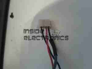
Red & Blue for power input, & a coax for the video. For the video GND connection, I have repurposed the Rec. LED input pin, putting a shorting link across where the LED would go to create a link to signal ground. Keeping this separate from the power GND connection reduces noise on the CRT.

Viewfinder CRT Assembly

Here’s the complete assembly liberated from it’s plastic enclosure.

PCB Closeup
PCB Closeup

Closeup of the control PCB. The 3 potentiometers control the CRT brightness, focus & vertical size.

M01KGG007WB CRT
M01KGG007WB CRT

The tiny CRT. Only ~60mm in length, with an 18mm screen size. This tube runs on +2294v final anode voltage. Much higher than I expected.

Electron Gun Closeup

The electron gun assembly, with the cathode, focus & final anode cups.

Phosphor Screen
Phosphor Screen

This screen is just a little bigger than a UK 5p piece! A marvel of precision engineering.


Posted on Leave a comment

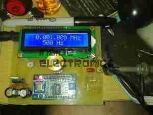
AD9850 VFO Board

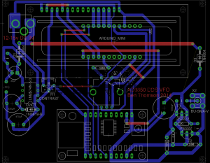
Continuing from my previous post where I published an Eagle design layout for AD7C‘s Arduino powered VFO, here is a completed board.

I have made some alterations to the design since posting, which are reflected in the artwork download in that post, mainly due to Eagle having a slight psychotic episode making me ground one of the display control signals!

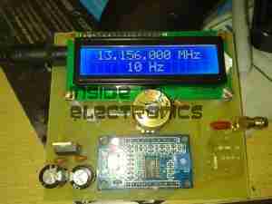
AD9850 VFO
AD9850 VFO

The amplifier section is unpopulated & bypassed as I was getting some bad distortion effects from that section, some more work is needed there.
The Arduino Pro Mini is situated under the display, and the 5v rail is provided by the LM7805 on the lower left corner.

Current draw at 12v input is 150mA, for a power of 1.8W total. About 1W of this is dissipated in the LM7805 regulator, so I have also done a layout with an LM2574 Switching Regulator.
The SMPS version should draw a lot let power, as less is being dissipated in the power supply, but this version is more complex.

DDS VFO-SMPS
DDS VFO-SMPS

Here the SMPS circuit can be seen on the left hand side of the board, completely replacing the linear regulator.
I have not yet built this design, so I don’t know what kind of effect this will have on the output signal, versus the linear regulator. I have a feeling that the switching frequency of the LM2574 (52kHz) might produce some interference on the output of the DDS module. However I have designed this section to the standards in the datasheet, so this should be minimal.

Nevertheless this version is included in the Downloads section at the bottom of this post.

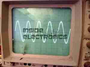
The output coupled through a 100nF capacitor is very clean, as can be seen below, outputting a 1kHz signal. Oscilloscope scale is 0.5ms/div & 1V/div.

VFO Output
VFO Output (Mucky ‘Scope)
Scope Connected
Scope Connected


Thanks again to Rich over at AD7C for the very useful tool design!

Linked below is the Eagle design files for this project, along with my libraries used to create it.

[download id=”5571″]

[download id=”5573″]

[download id=”5575″]

Posted on Leave a comment

4″ 7-Segment Display Driver

I was recently given some 4″ 7-Segment displays, Kingbright SC40-19EWA & of course, I needed to find a use for them.

I only have three, so a clock isn’t possible…

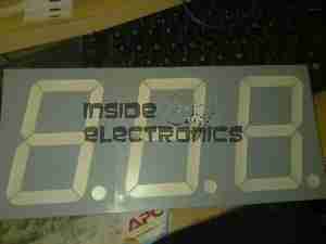
4" 7-Segment Display
4″ 7-Segment Display

As these displays are common cathode, & have a ~9v forward voltage on the main segments, some driver circuity is required to run multiplexed from an Arduino.

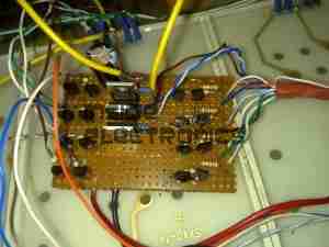
Driver Transistors
Driver Transistors

Driver circuit built on Veroboard, PNP segment transistors on the left, cathode NPN transistors in the centre, level-shifting NPN array on the right.

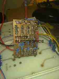
Base Bias Resistor Network

Base bias resistors on the back of the board to bias the bases of the segment drive transistors correctly.

Display Rear
Display Rear

Board soldered into the pins of the displays, which have been multiplexed.

Schematic to come along with some Arduino code to run a room thermometer, with an LM35 sensor

Posted on Leave a comment

LM386 Stereo Audio Amplifier

The quickest project from inception to working PCB yet:

From inception to a working PCB took only 4 hours!

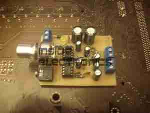
LM386 Amplifier
LM386 Amplifier

This is a miniature stereo audio amplifier, 0.5W per channel, that can be run from any voltage between 4-12v DC.

As usual, all the Eagle project files are available for download below & kits/bare PCBs will be available for sale for those that cannot etch boards.

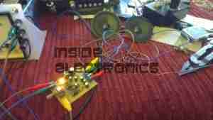
In Operation
In Operation

Here is the circuit driving a pair of 3W 8Ω speakers from a line level audio source. The gain of this circuit is set at 50 with the components specified.


Schematic
Schematic

As can be seen from the schematic, this is a pair of single LM386 ICs for each channel.

Gain can be set by altering R3 & R4

[download id=”5566″]

Buy Kits Here £9.50:
[wp_cart_button name=”LM386 Stereo Audio Amplifier Kit” price=”9.50″]

Buy bare PCBs here £5:
[wp_cart_button name=”LM386 Stereo Audio Amplifier PCB” price=”5″]

PCBs are etched on FR4 laminate with 8oz copper with top component silkscreen.

Posted on 1 Comment

AVR Optical Tachometer

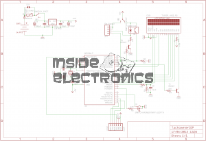
Here is an AVR powered optical tachometer design, that I adapted from the schematic found here.

I made a couple of changes to the circuit & designed a PCB & power supply module to be built in. The original design specified a surface mount IR LED/Photodiode pair, however my adjustment includes a larger IR reflectance sensor built onto the edge of the board, along with a Molex connector & a switch to select an externally mounted sensor instead of the onboard one.

There is also an onboard LM7805 based power supply, designed with a PCB mount PP3 battery box.
The power supply can also be protected by a 350mA polyfuse if desired. If this part isn’t fitted, then a pair of solder bridge pads are provided within the footprint for the fuse to short out the pads.

For more information on the basic design, please see the original post with the link at the top of the page.

Schematic
Schematic

Here is an archive of the firmware & the Eagle CAD files for the PCB & schematic design.


Posted on Leave a comment

Ultracapacitor Charge Balancing

Balancer
Balancer

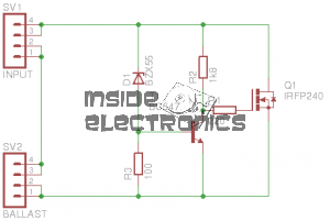
I have finally  got round to designing the balancing circuitry for my ultracapacitor banks, which have a total voltage of 15v when fully charged. The 2600F capacitors have a max working voltage of 2.5v each, so to ensure reliable operation, balancing is required to make sure that each capacitor is charged fully.

The circuit above is a simple shunt regulator, which uses a 2.2v zener diode to regulate the voltage across the capacitor.

A 10W 1Ω resistor is connected to the BALLAST header, while the capacitor is connected across the INPUT. Once the voltage on the capacitor reaches 2.6v, the MOSFET begins to conduct, the 1Ω resistor limiting current to ~2.6A.

Each capacitor in the series string requires one of these connected across it.

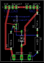
PCB
PCB

Below is a link to the Eagle project archive for this. Includes schematic, board & gerber files.

[download id=”5555″]

Posted on 1 Comment

Velleman MK179

Completed Kit
Completed Kit

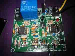
This is the Velleman MK179 Proximity Card Reader, which is supplied in kit form. In the image above you can see the completed kit, the read coil is etched onto the black PCB on the left. Bringing a recognised card close to the coil operates the relay on the main PCB for a programmable amount of time.

Main PCB
Main PCB

Closeup of the main PCB, 12v DC input at top right. Left IC is an LM358 dual Op-Amp, the IC on the right is a PIC12F629 with Velleman’s custom firmware.
Logic power is supplied to the ICs & the oscillator from the LM7805 regulator at the top of the PCB. The relay is a standard 15A SPDT 12v coil relay, with the switch contacts broken out onto the screw terminals on the left.

Schematic Diagram
Schematic Diagram

As it is not provided with the kit, unlike other Velleman kits, here is the schematic for this.


Posted on 5 Comments

Rare Veroboard Design Tools – Stripboard Magic

Stripboard Magic

Stripboard Magic is a Windows application for designing PCB layouts on stripboard (aka prototyping board, aka Veroboard). It was released by a British company called Ambyr which ceased trading a long time ago.

The interface is a quite primitive and a little strange but the program is functional even on Windows XP. It also works great under wine in Linux, at least with version 0.9.38 and above as this is all I have checked. It should probably work on older versions too. I haven’t tried it on Vista though.

It can be a handy program when called upon and I have successfully used it a few times when throwing together random small circuits. Due to the interface I would imagine it to be a bit clumsy for very large circuits. The biggest gripe I have with it is the inability to change the orientation of components on the board, so some circuits tend to be slightly larger than they need to be.

I downloaded a copy of Stripboard Magic 1.0 back in the 90’s and recently just found it lying about on my computer. As I would consider it to well and truly be abandonware and as it seems to be a little sought after by some hobbyists I have provided a link to download it below.

[download id=”5624″]

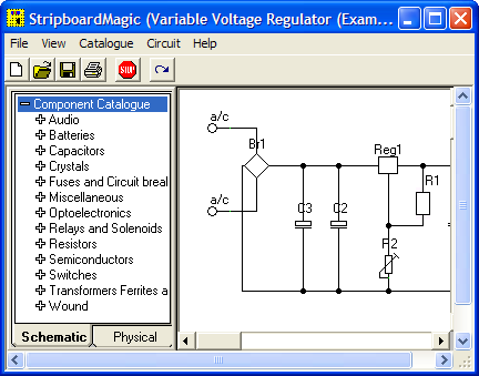
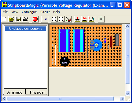
Here are some screenshots showing the schematic view (top) and board layout view (bottom):


Stripboard Designer

Another hard to find app these days is Stripboard Designer, mirrored here for people who wish to use it.

[download id=”5626″]

[download id=”5628″]

Posted on Leave a comment

Laser Diode Driver

Connection

Closeup
Closeup

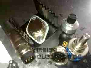
The parts arrived for my adjustable laser diode driver! Components here are an LM317K with heatsink, 100Ω 10-turn precision potentiometer, 15-turn counting dial & a 7-pin matching plug & socket.

Driver Schematic
Driver Schematic

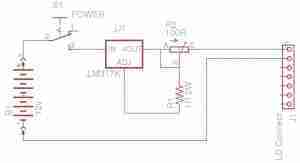
Here is the schematic for the driver circuit. I have used a 7-pin socket for provisions for active cooling of bigger laser diodes. R1 sets the maximum current to the laser diode, while R2 is the power adjustment. This is all fed from the main 12v Ni-Cd pack built into the PSU. The LM317 is set up as a constant current source in this circuit.

Installed
Installed

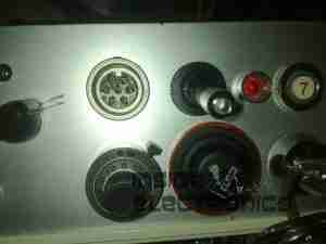
Here the power adjust dial & the laser head connector have been installed in the front panel. Power is switched to the driver with the toggle switch to the right of the connector.

Regulator
Regulator

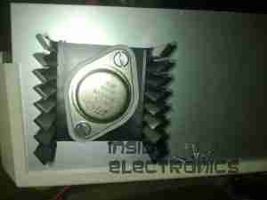
The LM317 installed on the rear panel of the PSU with it’s heatsink.

Connection
Connection

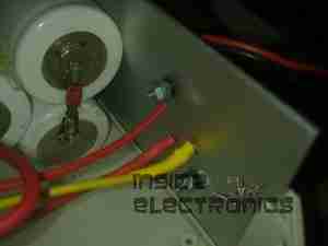
Connections to the regulator, the output is fully isolated from the heatsink & rear panel.