Posted on Leave a comment

Etching PCBs With Dry Film Photoresist

Since I do my own PCBs on a somewhat regular basis, I decided it was time to move to a more professional method to etch my boards. I have been using the cheap toner transfer method, using special yellow coated paper from China. (I think it’s coated in wax, or some plastic film).

The toner transfer paper does usually work quite well, but I’ve had many issues with pinholes in the transfer, which cause the etched tracks to look horrid, (not to mention the potential for breaks & reduced current capacity), and the toner not transferring properly at all, to issues with the paper permanently fusing to the copper instead of just transferring the toner.

BigClive has done a couple of fairly comprehensive videos on the dry film photoresist available from AliExpress & eBay. This stuff is used similarly to the toner transfer method, in that the film is fused to the board with heat, but then things diverge. It’s supplied either in cut sheets, or by the roll. I ordered a full roll to avoid the issues I’ve heard of when the stuff is folded in the post – once it’s creased, it’s totally useless. The dry film itself is a gel sandwiched between two protective plastic film sheets, and bonds to the board with the application of heat from a laminator.

The board is first cleaned with scotchbrite pad & soap to remove any tarnish & oil from the copper.
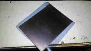
Dry Film
Dry Film

Once the board has been cleaned, one side of the backing film is removed from the gel with adhesive tape, and the dry film is placed on the board while still wet. This stops the film from sticking immediately to the clean copper, one edge is pressed down, and it’s then fed through a modified laminator:
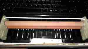
Modified Laminator
Modified Laminator

I’ve cut away most of the plastic covering the hot rollers, as constant jamming was an issue with this cheapo unit. All the mains power is safely tucked away under some remaining plastic cover at the end. The board with it’s covering of dry film is fed into the laminator – the edge that was pressed down first. This allows the laminator to squeeze out any remaining water & air bubbles from between the two so no creases or blisters form.
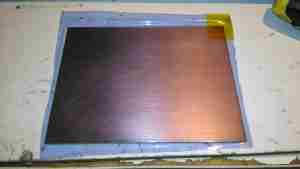
After Lamination
After Lamination

Once the board has been run through the laminator about 6 times, (enough to get it very hot to the touch), the film is totally bonded to the copper. The top film is left in place to protect the UV sensitive layer during expsure.
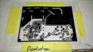
Photomask
Photomask

The exposure mask is laser printed onto OHP transparencies, in this case I’ve found I need to use two copies overlaid to get enough opacity in the black toner sections to block the UV light. Some touching up with a Sharpie is also easy to do if there are any weak spots in the toner coverage. This film is negative type – All the black areas will be unexposed and washed off in the developer tank. I also found I had to be fairly generous with track spacing, using too small lines just causes issues with the UV curing bits of film it isn’t supposed to.
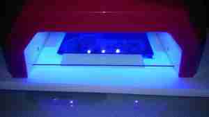
Exposing The PCB
Exposing The PCB

The PCB is placed on a firm surface, the exposure mask lined up on top, and the whole thing covered with a sheet of standard glass to apply even pressure. The UV exposure lamp in this case is a cheap eBay UV nail curing unit, with 15 high power LEDs. (I’ll do a teardown on this when I get some time, it’s got some very odd LEDs in it). Exposing the board for 60 seconds is all the time needed.
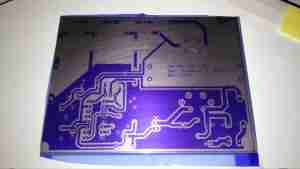
After Exposure
After Exposure

After the board is exposed, the areas that got hit with the UV light have turned purple – the resist has hardened in these areas. It’s bloody tough as well, I’ve scrubbed at it with some vigour and it doesn’t come off. Toner transfer was a bit naff in this respect, most of the time the toner came off so easily that the etchant lifted it off. After this step is done, the remaining protective film on the top can be removed.
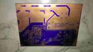
After Developing
After Developing

The film is developed in a solution of Sodium Carbonate (washing Soda). This is mildly alkaline and it dissolves off the unexposed resist.
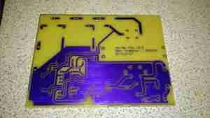
After Etching
After Etching

Now it’s into the etching tank for a couple of minutes, I’m still using Ferric Chloride to etch my boards, at about 60°C. Etching at room temperature is much too slow. Once this is done, the board is washed, and then dipped in the strip tank for a couple of minutes. This is a Sodium Hydroxide solution, and is very caustic, so gloves are required for this bit. Getting Ferric Chloride on skin is also a fairly bad idea, it stains everything orange, and it attacks pretty much every metal it comes into contact with, including Stainless Steel.

This method does require some more effort than the toner transfer method, but it’s much more reliable. If something goes wrong with the exposure, it’s very easy to strip the board completely & start again before etching. This saves PCB material and etchant. This is definitely more suited to small-scale production as well, since the photomask can be reused, there’s much less waste at the end. The etched lines are sharper, much better defined & even with some more chemicals involved, it’s a pretty clean process. All apart from the Ferric Chloride can be disposed of down the sink after use, since the developer & stripper are just alkaline solutions.
 

Posted on 3 Comments

Arduino Based SWR/PWR Meter – The Board

I recently posted about a small analog SWR/Power meter I got from eBay, and figured it needed some improvement.

After some web searching I located a project by ON7EQ, an Arduino sketch to read SWR & RF power from any SWR bridge.
The Arduino code is on the original author’s page above, his copyright restrictions forbid me to reproduce it here.

I have also noticed a small glitch in the code when it is flashed to a blank arduino: The display will show scrambled characters as if it has crashed. However pushing the buttons a few times & rebooting the Arduino seems to fix this. I think it’s related to the EEPROM being blank on a new Arduino board.

I have run a board up in Eagle for testing, shown below is the layout:

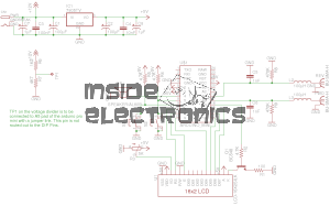
SWR Meter SCH
SWR Meter SCH

The Schematic is the same as is given on ON7EQ’s site.
Update: ON7EQ has kindly let me know I’ve mixed up R6 & R7, so make sure they’re switched round when the board is built ;). Fitting the resistors the wrong way around may damage the µC with overvoltage.

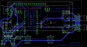
SWR Meter PCB
SWR Meter PCB

Here’s the PCB layout. I’ve kept it as simple as possible with only a single link on the top side of the board.

PCB Top
PCB Top

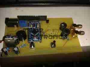
Here’s the freshly completed PCB ready to rock. Arduino Pro mini sits in the center doing all the work.
The link over to A5 on the arduino can be seen here, this allows the code to detect the supply voltage, useful for battery operation.
On the right hand edge of the PCB are the pair of SMA connectors to interface with the SWR bridge. Some RF filtering is provided on the inputs.

PCB Bottom
PCB Bottom

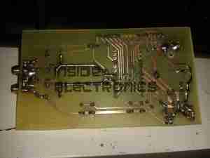
Trackside view of the PCB. This was etched using my tweaked toner transfer method.

LCD Fitted
LCD Fitted

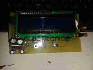
Here the board has it’s 16×2 LCD module.

Online
Online

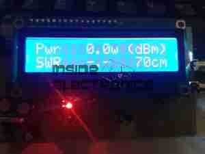
Board powered & working. Here it’s set to the 70cm band. The pair of buttons on the bottom edge of the board change bands & operating modes.
As usual, the Eagle layout files are available below, along with the libraries I use.

[download id=”5585″]

[download id=”5573″]

More to come on this when some components arrive to interface this board with the SWR bridge in the eBay meter.

Posted on 4 Comments

AD9850 DDS VFO PCB & Schematic Layout

I recently came across a design for an Arduino controlled AD9850 DDS module, created by AD7C, so I figured I would release my Eagle CAD design for the PCB here.

It is a mainly single-sided layout, only a few links on the top side are needed so this is easy to etch with the toner transfer method.

My version uses an Arduino Pro Mini, as the modular format is much easier to work with than a bare ATMega 328.

RF output is via a SMA connector & has a built in amplifier to compensate for the low level generated by the DDS Module.

DDS VFO
DDS VFO

Version 2 Update: Added reverse polarity protection, added power indicator LED, beefed up tracks around the DC Jack.
[download id=”5571″]

Posted on Leave a comment

555 Flyback Driver

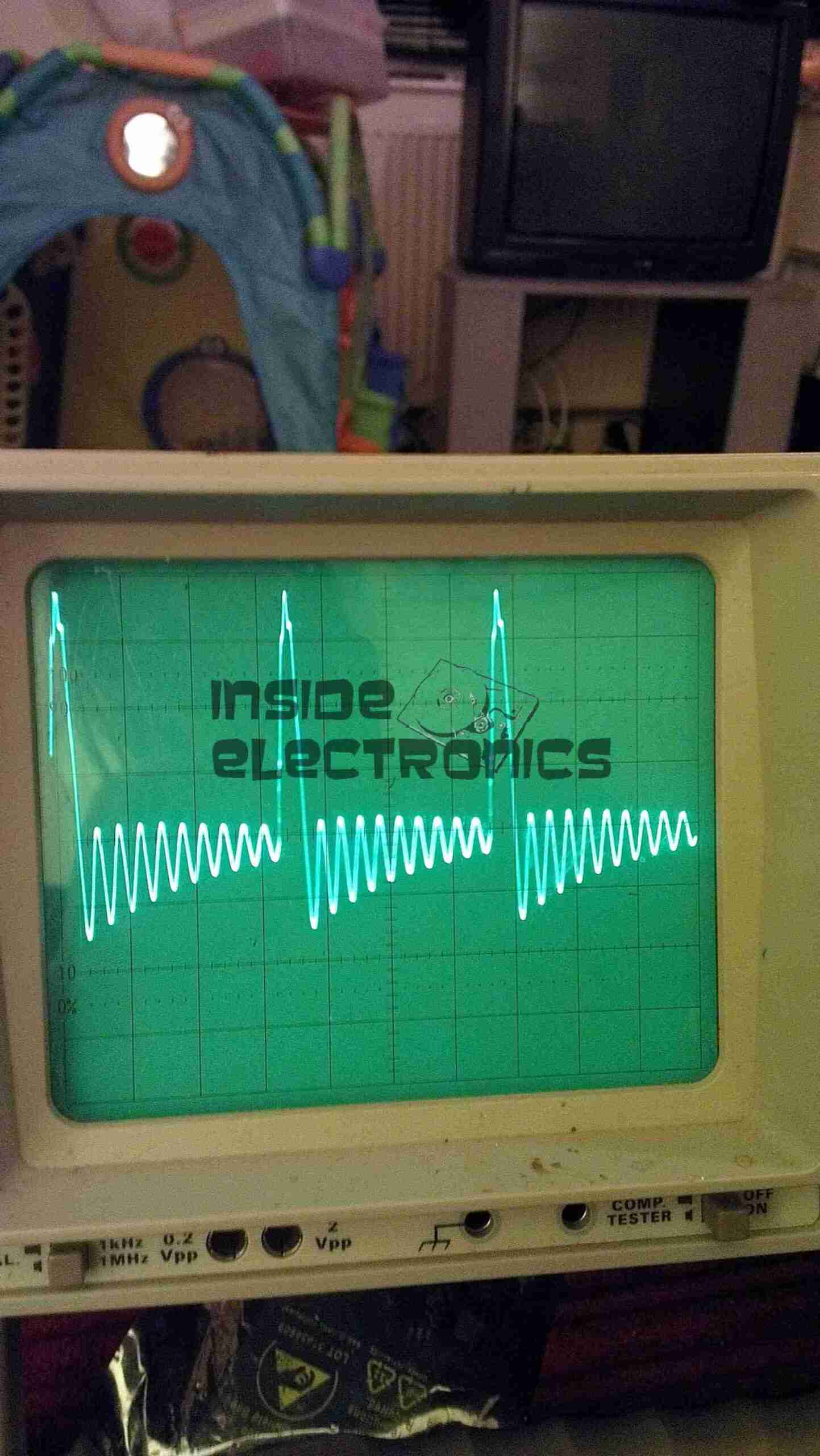
Flyback Secondary Waveform
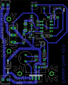
Board Layout
Board Layout

Here is a simple 555 timer based flyback transformer driver, with the PCB designed by myself for some HV experiments. Above is the Eagle CAD board layout.

The 555 timer is in astable mode, generating a frequency from about 22kHz to 55kHz, depending on the position of the potentiometer. The variable frequency is to allow the circuit to be tuned to the resonant frequency of the flyback transformer in use.

This is switched through a pair of buffer transistors into a large STW45NM60 MOSFET, rated at 650v 45A.

Input power is 15-30v DC, as the oscillator circuit is fed from an independent LM7812 linear supply.

Provision is also made on the PCB for attaching a 12v fan to cool the MOSFET & linear regulator.

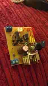
Initial Board
Initial Board

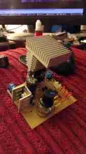
Board initially built, with the heatsink on the linear regulator fitted. I used a panel mount potentiometer in this case as I had no multiturn 47K pots in stock.

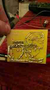
PCB Traces
PCB Traces

Bottom of the PCB. The main current carrying traces have been bulked up with copper wire to help carry the potentially high currents on the MOSFET while driving a large transformer.
This board was etched using the no-peel toner transfer method, using parchement paper as the transfer medium.

MOSFET Heatsinked
MOSFET Heatsinked

Main MOSFET now fitted with a surplus heatsink from an old switchmode power supply. A Fan could be fitted to the top of this sink to cope with higher power levels.

Gate Drive Waveform
Gate Drive Waveform

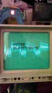
This is the gate drive waveform while a transformer is connected, the primary is causing some ringing on the oscillator. The waveform without an attached load is a much cleaner square wave.

Flyback Secondary Waveform

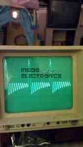
I obtained a waveform of the flyback secondary output by capacitively coupling the oscilloscope probe through the insulation of the HT wire. The pulses of HV can be seen with the decaying ringing of the transformer between cycles.

Corona Discharge
Corona Discharge
Arc Discharge
Arc Discharge

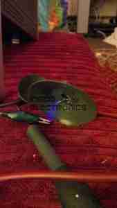
Corona & arc discharges at 12v input voltage.

Download the Eagle schematic files here: [download id=”5561″]